The schematics
The schematics, page 1 and 5.
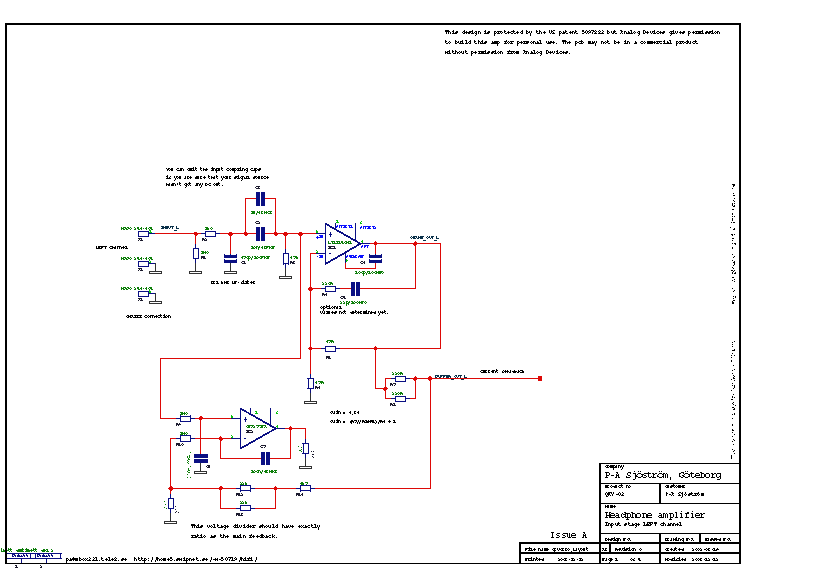
Click on the picture to get a larger view. The picture shows the schematics of the amp. Of course you can't use it for anything except for an overview. Please download the pdf-file instead if you want to see the details.
Circuit description
Before you read this please read the application note AN-211. I have a copy which is scanned better than the original.
AN-211, original at Analog Devices
AN-211, better quality at a my web site.
The very original
I have also the original article of Mr. Mark Alexander from the Journal of Audio Society. The original article is not much different from the AN-211 but the AN-211 is a bit edited to suit as an application note. I recommend though that you read this AN-211 first in order to understand the patented design.
The front-end opamp
The amp consists of two main parts. One front-end which is an opamp, IC1. The other main part is a transimpedance amplifier (current feedback amplifier, CFB). Instead of tying T1 and T2 together and get a conventional CFB amp I have insert an opamp as the front-end. This is the patent, using an opamp in this particular position.
The opamp creates a high impedance input and a extremely low distortion driver. Further more you will get extremely low noise if the opamp is of such kind. Almost any good opamp will fit in this application and the opamp don't have to be so fast because the speed is increased in this circuit. The opamp has the output connected to a heavy load down to ground. This load creates extra supply currents through pin 4 and 7 of the opamp. This DC current plus signal current is fed to a current mirror and buffered by a diamond buffer. The current mirror and the buffer are designed nearly exactly the same as QRV-06. This CFB amp is designed to be very fast, around 20MHz bandwidth.
The "speed increase" is set by the gain around the opamp.R5/R6 + 1. In my case gain is 2 which means that the opamp will be two times faster than normal. The total gain is set by (R7//R8+R5)/R6 + 1.
C4 is only for the LT1115 or LT1028 opamp. If you choose an another opamp you must leave this place (C4) empty.
R4 and C5 are "just in case" parts. They are not used.
The DC servo
The input opamp is very good when it comes to input offset voltage but in this topology you have one more source for output offset. This offset can't be removed by the input opamp. The offset is caused by mismatch of the current mirrors, T3, T5 and T4, T6. To romeve this current mirror offset you must a DC servo which in this case has a little bit odd connection. The servo senses both the input signal and the output signal.
It's very important that the ratio of the voltage divider (R11-R14) of the servo is exactly the same as for the main feedback (R5-R8). If not you will not get low output offset. I have chosen to have the servo feedback exactly 100 times more than the main feedback. R12-R14 simulates the main feedback. This was an easy way to create accurancy. The output of the servo is more current consumption caused by R15. The output signal of both opamps appears on the supply pins, pin 4 and 7.
The schematics, page 4, 3
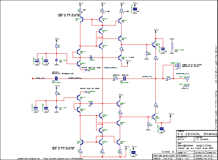
Click on the picture to get a larger view. The picture shows the schematics of the amp. Of course you can't use it for anything except for an overview. Please download the pdf-file instead if you want to see the details.
The transimpedance amp, CFB amp or current feedback amp
This amp look very complicated but it isn't if you can identy the different parts. First, compare the QRV-06. This section is almost identical with QRV-06.
The amp hasn't got any non-inverting inputs. The bases of T1 and T2 is held on a fixed potential. This potential is also the supply voltage of the main opamp IC1. The zeners are 9.1 volts which means that the opamps will get 8.4-8.5 volts as supply voltage.
T19, T21 (connected as a diode), D9 and D10 are anti-saturation parts when the amp is clipping.
Wilson current mirrors
The amp has only got inverting inputs and those are the emitters of T1 and T2. The error signal (input-output) comes out from the opamps supply pins, pin 4 and 7. This DC current plus AC signal is fed through the emitters and comes out at the collector more or less a copy of the emitter current. This current is fed to a Wilson current mirror which is a current mirror with a cascode. The mirror is formed by T3, T5, T9, R18 and R20. T7 creates only a DC shift and let the T11 have a little bit more collector voltage.
You pay some attention to R18 and R19. The amp is designed to have 1 volt over these resistors. If you change opamps you may be forced to trim thse values. Luckely it isn't very critical when you change the working bias for a CFB amp. LT1115 plus OPA227 comsume 8 mA (my protoype) and OPA134 plus OPA227 consume 4 mA. So if you use OPA134 R17, R18 may be changed to 220 or 270 ohms.
The output diamond buffer
The output from this current mirror is the high impedance node, the collectors of T9 and T10. The impedance is in the aera of a couple of megaoghms. This very high output impedance output must iof course be buffered. For this I have chosen to have a classical diamond buffer. See SSB-01. This buffer is enhanced with cascoded current sources which makes a very low distortion buffer. The whole buffer is good for towards 100 MHz if the signal source would have been low ohmish.
Class A resistors, IMPORTANT, READ IT.
R26 and R27 must not be used. They are for class A mode and if this happen to be interesting the whole buffer must be redesigned. If they are soldered in you will get "notches" when the transistors go into class B. These notches are the same as nasty distortion. If you want to exeperiment make sure that you always have current through these resistors regardless of output signal and load.
With J1 you can drive your headphones with very low output impedance or with 100 ohms. This will in some case have influence of the sound.
C16, C17, R31 are for frequency compensation. They seems right now not being necessary.
The schematics, page 2
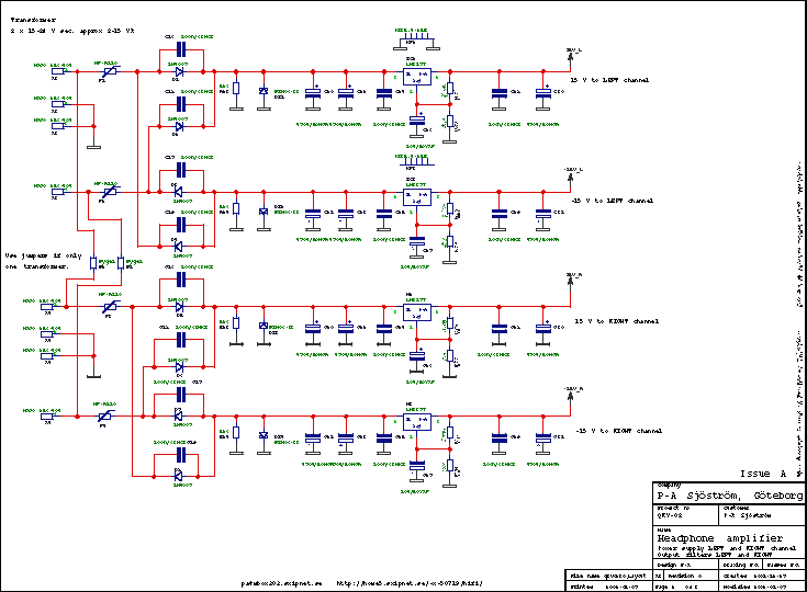
Click on the picture to get a larger view. The picture shows the schematics of the amp. Of course you can't use it for anything except for an overview. Please download the pdf-file instead if you want to see the details.
The power supply
The power supply is rather simple using LM317 and LM337. Those regulators are quite good, not as bad as the reputation. They are set to 18 volts in order to maximize the output signal. The CFB amp looses rather much due to the cascodes. The exact value for the voltage setting resistors are 220 ohms and 3.0 kohms. If you don't can get this value you can use 3.3 plus 33 kohms instead.
R32, R33 serves as bleeder resistors and the prurpose is a controlled power down.
DZ1, DZ2 is just for absorbing transisents coming from the mains and the transformers. They may not be necessary.
