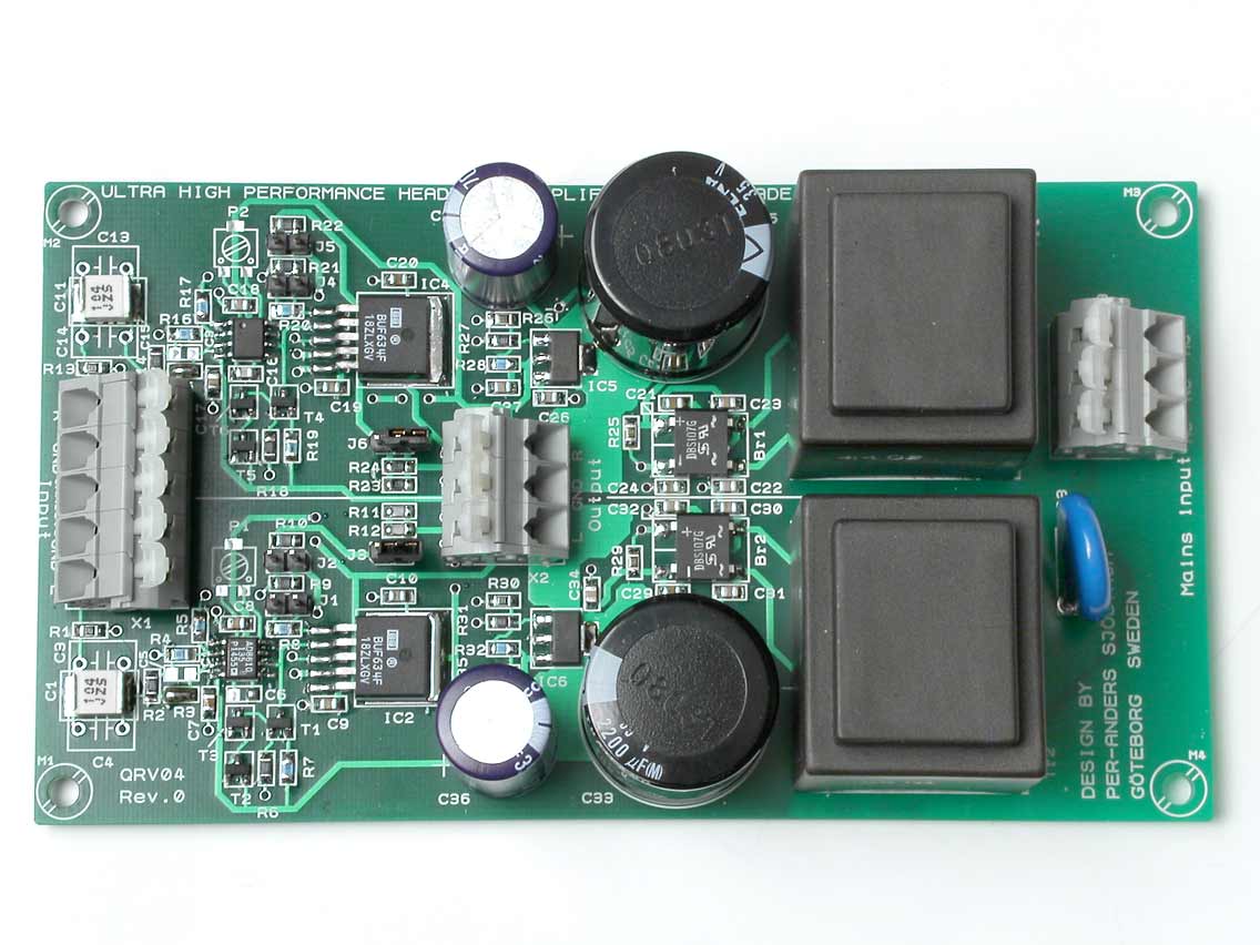
QRV-04 - The high performance SMD headphone amplifier with multiple feedback
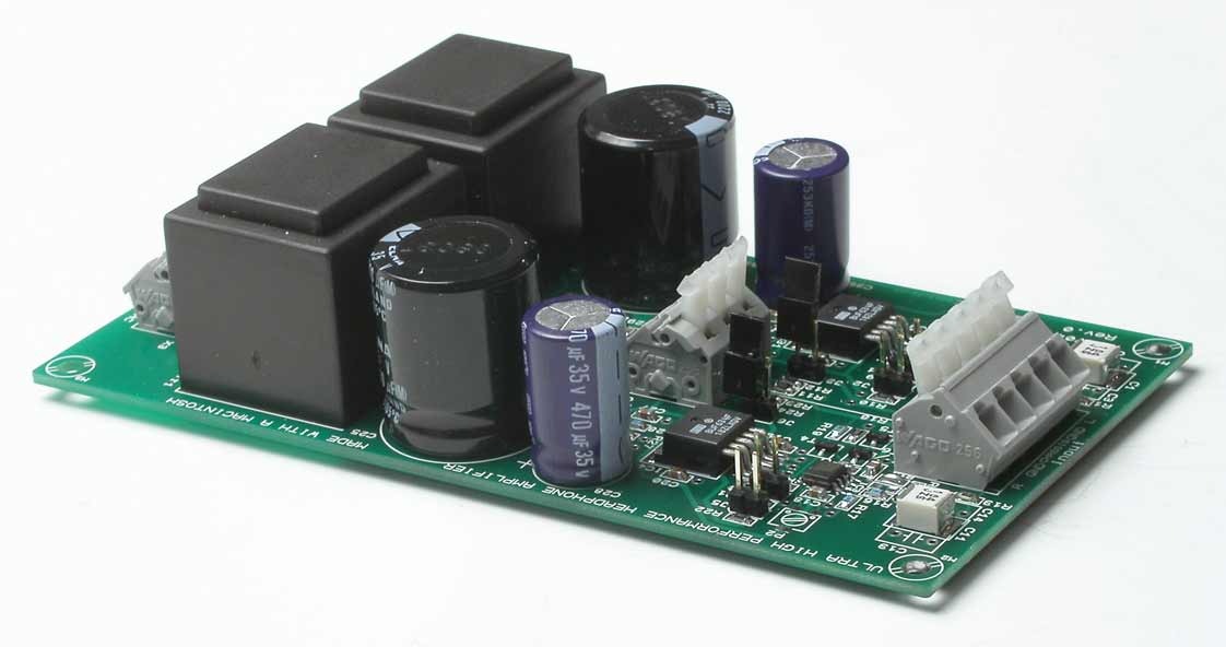
Click on the picture to see a preview of the pcb.
Interesting features:
- The pcb fits virtually any single opamp with or without offset trim.
- Room for good coupling caps (if you must or like), both SMD and regular hole mounted, if you are having trouble in finding big SMD caps.
- Input LP-filter if you have problems with RF interference (you should have a filter though).
- Room for DC removal cap (if you need this).
- Crossover distortion reducer for the opamp. This is a popular circuit in the DIY community.
- Current limitation inside the feedback loop (choose the value you like)
- High speed and high performance SMD buffer as output stage.
- Local feedback for stable performance (only if necessary).
- Multiple feedback as an option.
- High quality power supply with large smoothing caps and transformers on the pcb.
- Fits any headphone (except for electrostatic of course).
The background
Since many years back I make SMD designs at work but I have never before designed any audio with mainly SMD parts. This is my very first audio SMD project. Recently I have updated the design a bit. I have implemented a thing called "multiple feedback". Walt Jung has written an article in the subject.
The article can be found here.
This project is not suitable for a newbeginner, but if you only have a soldering iron with a very fine tip and you don't tremble and have a good pair of tweezers, it shouldn't be any problems to succeed. This amp is not very hard to solder, yes I'm not kidding and it's really cool, not common DIY stuff!
Active elements are AD8610 OPA134 or OPA627 and a buffer BUF634. The operational amplifiers are one of the best in their market segments. The AD8610 is new and very interesting.
The performance is outrageous in headphone amp terms. See the technical data!
My design goal was to make a simple but well balanced amp in terms of component choices and a well-tested topology.
The schematics
The schematics, page 1 and 3.
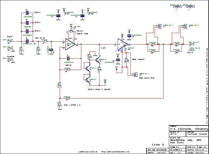
The picture shows the schematics of the amp. Of course you can't use it for anything except for an overview. Please download the pdf-file instead if you want to see the details.
The schematics, page 2
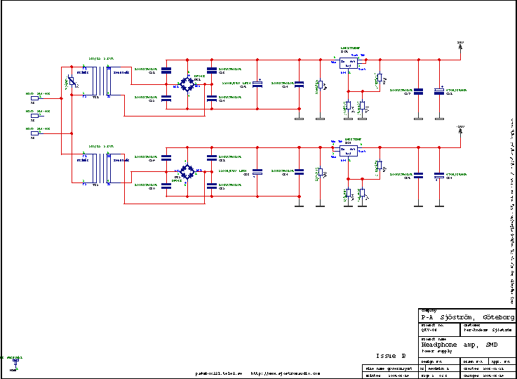
The picture shows the schematics of the amp. Of course you can't use it for anything except for an overview. Please download the pdf-file instead if you want to see the details.
Circuit description
The text is for the right channel.
*******************************
The main part, the operational amplifier
The main part is an operational amplifier, IC1. The opamp is followed by a high speed buffer capable of up to 250 mA which will be sufficient for all headphones on the market. In between the opamp and the buffer I have put a class A circuit, T1 and a few resistors around.T2 and T3 serves only as diodes and can be replaced with any diode or transistor connected as a diode(base and collector tied together, emitter= anode). This circuit will reduce the crossover distortion, but I don't know how much. You can omit the whole circuit if you don't experience any advantage.
Frequency compensation
C6 is for frequency compensation but is not required for most opamps. Fast opamps like OPA627may need this capacitor. Consult the datasheet of BUF634.
Offset voltage
P1 is only used if you don't use a precision opamp. OPA627 and AD8610 have so good offset values which make this potentiometer unnecessary. OPA134 is slightly worse but still good. Weather P1 should be used or not, consult the datasheet of the opamp. If you can, avoid these offset trimming pots. If you use them you will get worse temperature characteristics. Note also that you in this case only can use opamps which has this trimpot connect to positive supply voltage (most common).
Calculating the gain
The total gain is determined by R4 and R5. Gain = R5/R4 + 1. Low values of these resistors is important if you want low noise.
The input filter
The input filter is very universal. You should have a lowpass filter, R3 and C5, but if you don't have any RFI trouble at all, it's not necessary, just replace the R3 with a jumper and omit C5. DC blocking capacitor may be necessary but check with your signal source first. The whole amp is DC connected so you must ensure that you haven't got any DC in your signal. In order to be flexible I have made room for any type of input coupling capacitor, or capacitors. Since this is a SMD amp I recommend the SMD capacitor. I have chosen a type from RIFA but any "polypropulene compatible" type will do. R2 is very necessary if you use input couplings cap. The resistor creates a DC path for the inputs of the opamp, otherwise it won't work. R1 is a pulldown resistor so the input coupling capacitor won't pick up any charges when the amp is unconnected. A charge capacitor can creates a nasty spike at the output when something is connected to input.
The output buffer
The output buffer is a high speed integrated buffer which can be biased with different currents. I have chosen "medium speed" and "high speed". This is only for personal taste. High speed mode consumes rather much power and adds very little in audio quality but some fast opamps requires this mode in order to be stable. If you want to use this amp with batteries you should use "low speed mode", remove R8. This will exclude fast opamps like OPA627.
The output current limitation
R9, R10 or R11, R12 aren't necessary but those resistors creates current limitation which means that both low impedance och high impedance headphones can be connected. Without these resistors it's very easy to damage low impedance headphones but if you have full control over the situation, omit those resistors. I should mention that many headphones are designed to be driven from a certain source impedance. Some people claim that this impedance is 120 ohms. Test this if you want to optimize the listening experience. Using R9, R10 creates the possibilities to use long cables with no (or little) loss of the higher frequencies. R11, R12 is the classical way of driving headphones. I have made an option for changing "drive modes". With original cable lenght I can't hear any difference between these two modes. Some people claim huge differencies though.
The power supply
The power supply is not very exotic, rather straight forward. It's designed to use two transformers, one for the positive voltage and the other one for the negative.
The regulators are cooled by the groundplane and of a copper area on the upper side. If you plan to use AD8610 you must lower the voltage to 13 volts! AD8610 is made in a advanced high speed process which has 27.3 V as absolute maximum. I have used AD8610 for a while with +- 15 volts and the amp works still and will probably work but I don't recommend using the opamp beyond it's limits. Remove R27 and change R26 to 2.7 kohms. This will lower the voltage.
R25 is a bleeder resistor. The regulators won't discharge the capacitors completely when the have reached the voltage of 0,6 V. The resistor creates a clean start at power up.
C21-C24 are for reducing EMI caused by diode switching.
The transformers are short circuit proof by design, therefore you don't need fuses.
R33 is for transient suppression.
The pcb layout
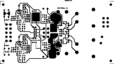
The component print
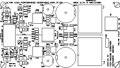
The picture shows the component print of the PCB. Of course you can't use it for anything except for an overview. Please download the pdf-file instead if you want to see the details.
The printed circuit board is made for two channels, contains everything, power supply and the amp itself, including transformers except for connectors. I have chosen not to have pcb mounted headphone and phono connectors because it's hard to fit in a case.
The pcb have groundplane on the lower (solder) side (not shown in pictures) which is essential in order to get good results.
The solder side
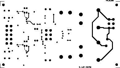
The picture shows the solder side of the PCB. Of course you can't use it for anything except for an overview. Please download the pdf-file instead if you want to see the details.
Almost everyone of the traces are on the solder side. The groundplane is very covering, only a few traces on the solder side.
The component side
The picture shows the component side of the PCB. Of course you can't use it for anything except for an overview. Please download the pdf-file instead if you want to see the details.
Almost everyone of the traces are on the component side as you can see. The groundplane is on the solder side.
The groundplane mask

The picture shows the groundplane mask of the PCB. Of course you can't use it for anything except for an overview. Please download the pdf-file instead if you want to see the details.
The black area is without groundplane and this is under the transformers.
The hot relief pads
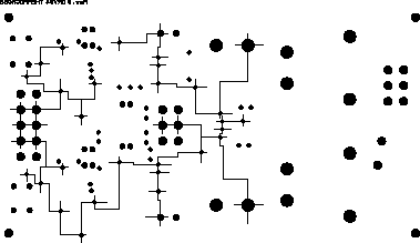
The picture shows the pads which are connected to groundplane of the PCB. Of course you can't use it for anything except for an overview. Please download the pdf-file instead if you want to see the details.
Each "cross" at the pads is a ground connection. This file is used together with the solder side in a sandwich. I use this technique because my cad program has a very slow groundplane generation.
Build directions
Click on the picture to see a preview of the pcb.
This design is very easy to build. You can of course solder everything and then apply voltage but maybe it doesn't hurt to be a little cautious. You should start with all low SMD parts except for the buffer and the opamp becuase it's harder to solder the SMD parts when you have big parts in the way. For this solder job I recommend a good pair of tweezers. I use a type especially made for SMD. With this tweezer I'll get a very good grip. You must also have a soldering iron with a small tip but at least 50 watts in order to be able to solder the buffer which requires lot's of heat.
Start with all low SMD parts except for buffer and opamp
- Resistors
Transistors
Trim pot (if you use it)
Capacitors, not the hole mounted ones
Rectifier bridges, at last - Then continue with the high electrolytic caps, mount all caps
- Connectors
- Jumpers
- Transformers
- Varistor
Check the power supply
Apply voltage, 230 volts AC. Check that the regulators give the expected voltage, +- 15 volts except when you plan to use AD8610. Disconnect the power and see to that the voltage is zero when you continue the soldering.
Continue with the opamp and buffer
- Opamp.
- Buffer. This parts needs to be soldered into the large pad on the pcb. To do this you must use lot's of heat. If you have two soldering irons, use both at the same time. The buffer gets it's cooling via this pad so it's important that the buffer is very good soldered.
Check the finished amp
Apply voltage again and check the output voltage. Measure the DC voltage at the output. It should be the specified offset voltage (see datasheet) and times the gain, 4 in this case. I got 78 uV(!) for AD8610, 2.56 mV for OPA134 and 0.7 mV for OPA627
Check voltage regulation
Connect the amp for high speed mode. The pcb and the transformers get hot (or at least warm) eventually. Check that the supply voltage still is +-15 volts or the value you have chosen.
The whole amp is ready.
Test if you want the different drive and speed modes. It is safe to change modes when voltage and input signal is applied. You won't even hear a click.
Good luck and happy listening.
Listening experience
How does it sound really? The protoype is built and it works real good.
I have used this amp for some time now and I must say as my little daugther says about everything (she "loves" all things or persons she likes. She doesn't know exactly what love means but she thinks it's the same as like), "I love this amp". It's totally transparent, like a polished daimond. I'm very influenced by the looks. I really like SMD. It's very cute. I have tested three different opamps AD8610, OPA134, OPA627 and I must say that I like AD8610 the most of some weird reason. I think I'm influenced of the pure and technical clean electrical performance. Step response is excellent and the offset voltage is extreme! Best I ever have come across. and
I'm not very good in expressing myself in english (not in swedish either) when it comes to listening impressions. I'd just LOVE this amp.
Technical data
Click on the picture to see a preview of the pcb.
| Frequency response: | 0 Hz - 1,5 MHz, -3 dB, OPA134 0 Hz - 5,0 MHz, -3 dB, OPA627 0 Hz - 6,0 MHz, -3 dB, AD8610 |
| Frequency response with input filter: | 7,2 Hz - 159 kHz, -3 dB |
| Power bandwidth at 10 Vrms, 50 ohms: | 0 Hz -250 kHz, -3 dB, OPA134 0 Hz -700 kHz, -3 dB, OPA627 0 Hz -700 kHz, -3 dB, AD8610 |
| Equivalent input noise: | 1,2 µV, OPA134 0,6 µV, OPA627 1,8 µV, AD8610 |
| Signal to noise ratio: | 116 dB, OPA134 122 dB, OPA627 113 dB, AD8610 |
| Dynamic headroom: | 136 dB, OPA134 142 dB, OPA627 133 dB, AD8610 |
| Distortion: | 0,00008 %, OPA134 0,00003 %, OPA627 0,00003 %, AD8610 |
| Slew rate: | 20 V/us, OPA134 55 V/us, OPA627 50 V/us, AD8610 |
| Step response: | Perfect without overshoot |
| Gain: | 4.1 (12 dB) |
| Input impedance: | 220 kohms |
| Output impedance: | 3 milliohms |
| Damping factor: | 16000 with 50 ohms load |
| Output current: | 250 mA peak |
| Supply voltage: | 230 V AC |
| Dimensions: | 76.2 (3.0") x 137.3 (5.4") mm |