QSX Mark II - The extreme phono (RIAA) amplifier
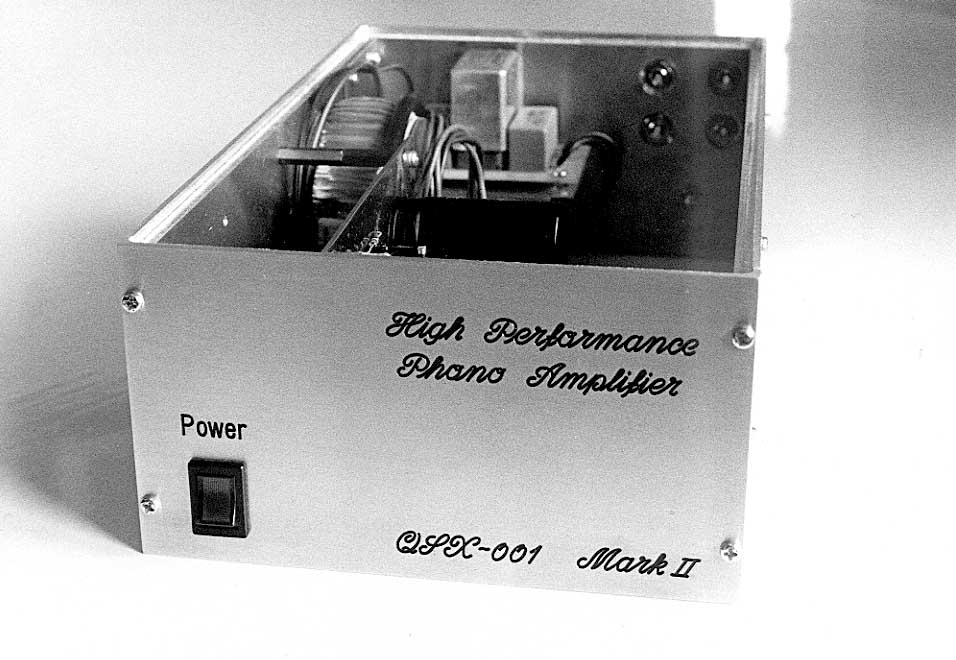
Click on the picture to get a larger view. The front view of the original QSX Amplifier from 1986. |
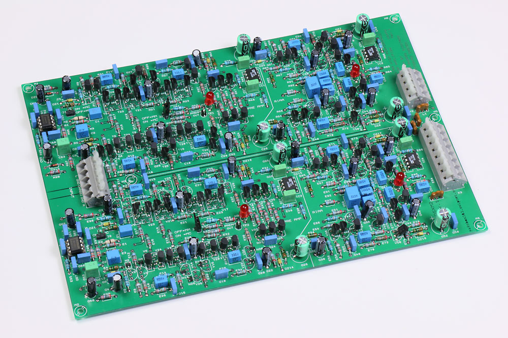
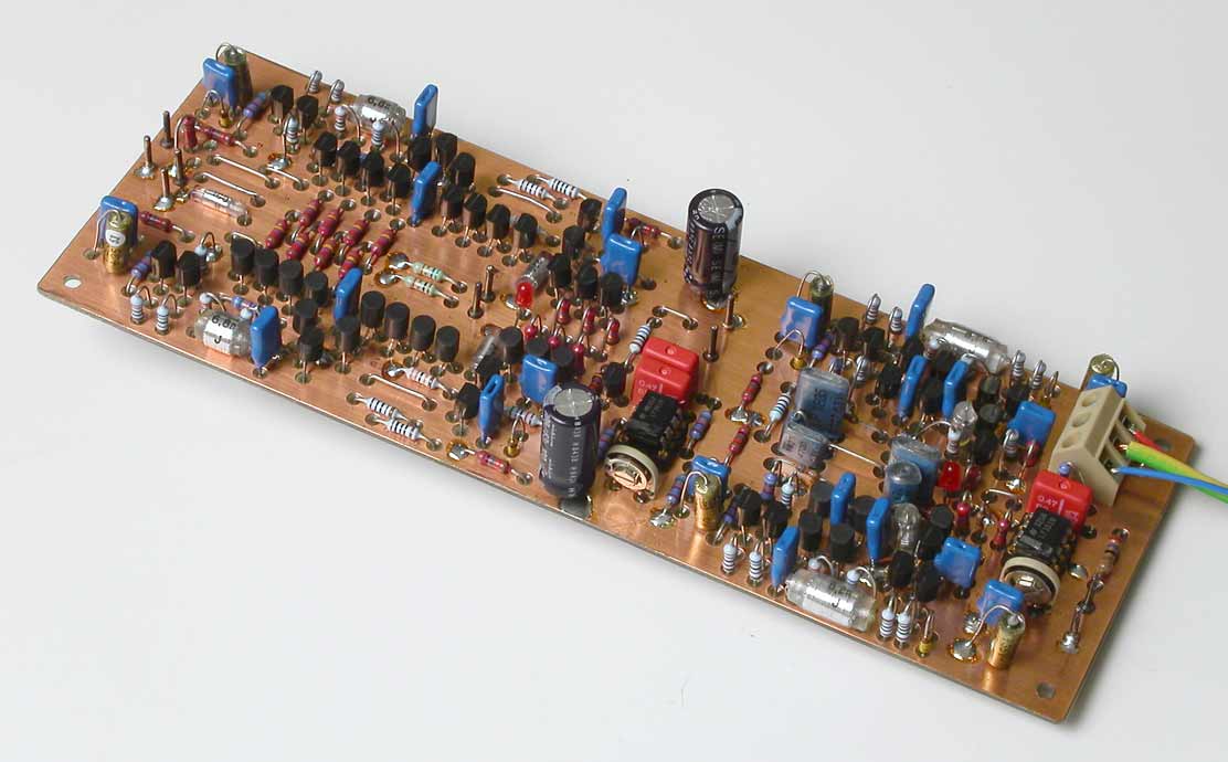
Click on the picture to get a larger view. The top view of the QSX Amplifier pcb. High resolution picture HERE. |
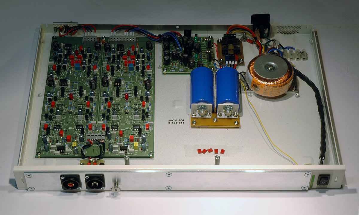
Click on the picture to get a larger view. This QSXM2 Amplifier built by a customer. The power supply is of an another brand. A good job, indeed and on top of, it he became very satisfied . |
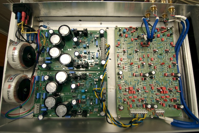
Click on the picture to get a larger view. This QSXM2 Amplifier built by an another customer. The power supply is QSXPS. Also here a very good job, indeed and this person became also very satisfied. |
The project has been very successful because everyone have succeeded. That is amazing if you take into account the huge amount of parts.
Interesting features
In order to get an extremely linear and extremely low distortion design I have taken a couple of measures:
- Symmetrical design
- No capacitors in the signal paths
- Cascodes in the input stage and in the high gain stage
- Buffered cascodes with emitter followers
- Possibility to use ultra low noise transistors
- High speed output stage
- Advanced input bias servo with chopper stabilized or conventional opamp
- Totally DC-coupled together with DC-servos and input bias current servo
- Many decoupling capacitors and EMI-filters
- Professional quality printed circuit board with groundplane
- The pcb has lot's of possibilities when it comes to tweaking. You could use JFET's as input transistors for instance.
Background
Click on the picture to get a larger view. The front view of the original QSX Amplifier.
Click on the picture to get a larger view. The original printed circuit board of the QSX Amplifier, only one channel.
A long time go
This phono amplifier design did I make a long time ago. The amp at the pictures has done service, almost every day since 1986! Good quality, isn't it? I'm very proud of it, despite the overkill, see down below. I got the inspiration of this paralleling technique of the input transistors from the magazine Elektor, some issue in the 80's but this fact has been known long before this.
Why did I design this amplifier?
Reason no. 1:
A friend of mine was searching for the perfect sound but not at any cost. He asked me to design an esoteric and orthodox moving magnet amplifier.
My friend had a turntable of a fairly good quality (changed from a Pioneer to a german Dual 505. He also switched the pickup to a better one (Ortofon VMS 20) but the sound quality wouldn't come. The sound was without life. The explanation was the built-in phono amp. This poor little amp was loaded with anti-emc stuff and the opamp was also a joke. The receiver was a simple model from Denon, rather good actually except of the phono amp.
My goal was to make a killer amp without to a very low cost. The performance should be outstanding! If you look at technical data maybe you agree.
Reason no. 2:
At that time I was a university student and I felt it was very interesting to combine theory with real life experience.
Reason no. 3:
17 years later I felt that the amp was rather timeless and worth publishing. Back then I didn't have the budget for making professional pcb's which I have now. I have had real fun when I soldered these industrial pcb's and it's looking nice too.
Reason no. 4:
Now 5 years later after my first internet publishing this amp is still my favorite. It represents for me a "timeless design".
VERY IMPORTANT:
This amp is an overkill and pure craziness, I know, but my friend and I are alone in having this unique amp (we are not alone anymore...). You can build a very good amp with NE5534, LT1115, LT1028, AD797, etc. to a fraction of the cost but it's not the same feeling. Why do some people like tubes? You know what I'm talking about.
It's a challenge to make the best possible sound quality there is with a minimum of components. It's very true if you want to sell the product and earn some money but on the other hand it's fun to ignore everything what's called sanity and live out your wildest dreams. Since I wrote this text I have created a design statement which I stay true to.
Although I agree to a certain extent what Mr. Nelson Pass says, I do believe that you get better results if you eliminate the bad behaviors of some components, transistors mainly. As always, if you know more about the inner life of the components, you'll get more control over the final result.
It was very fulfilling to have full control over the design process. All parameters, except the noise are determined by passive components only. I have tailored every detail in the performance. Every part in the amp have been thoroughIy analyzed and tested. I haven't tried to reduce the amount of components in order to get knowledge of what the component minimum are. After all the components are very cheap. I have used transistors for 3 cents!
At the left you can read a very true statement from Nelson Pass. (Take also a good look at his web site because he has lots of cool designs.)
This text comes from Nelson Pass at Pass Labs , and the A40 amp project:
The Pass A40 Power Amplifier
The Audio Amateur 4/78 by NELSON PASS
The schematic
The schematic, page 1 and 3, the pre amplifier
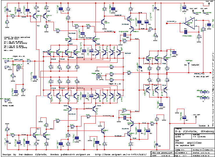
The picture shows the pre amp, page 1 and 3 of the schematic. Of course you can't use it for anything except for an overview. Please download the pdf-file instead if you want to see the details.
If you want a general description of the design, see the text down below.
The schematic, page 2 and 4, the RIAA amplifier
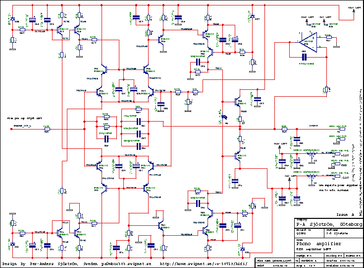
The picture shows the correction amp, page 2 and 4 of the schematic. Of course you can't use it for anything except for an overview. Please download the pdf-file instead if you want to see the details.
If you want a general description of the design, see the text down below.
The schematic, page 7, the servos
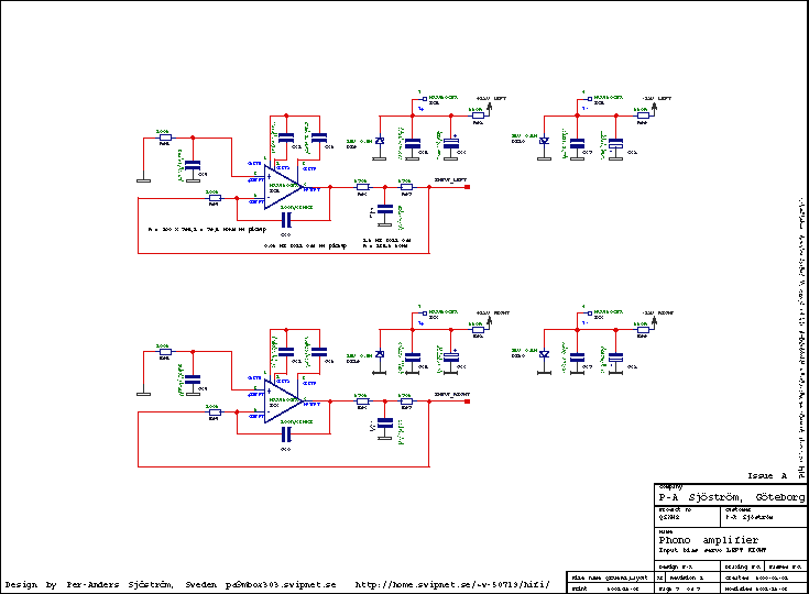
The picture shows the input bias servos, page 7 of the schematic. Of course you can't use it for anything except for an overview. Please download the pdf-file instead if you want to see the details.
Circuit description
The amp consist of two main parts, a preamp and a correction amp.
The preamp (see above and pdf-files ) has very low noise and an extremely flat frequency response, up in the megahertz-region. The input impedance is determined by the input bias servo. With the chosen resistor values the input impedance is 270 kohms. It's very easy to tailoring the input characteristics in order to fit any pickup. With resistors and capacitors, you can choose the input characteristics in the way you want.
The RIAA-amp amplifies the signal even more and then correct it according to the international RIAA-curve. The bass drop under 20 Hz isn't implemented. Unfortunately the input impedance of the RIAA-amp is low, only 680 ohms, but this compensates with the extremely low output impedance of the preamp, only 800 microohms.
In order to get an extremely linear and extremely low distortion design I have taken a couple of measures:
- Symmetrical design
- No capacitors in the signal paths
- Cascodes in the input stage and in the high gain stage
- Buffered cascodes with emitter followers
- Possibility to use ultra low noise transistors
- High speed output stage
- Advanced input bias servo with chopper stabilized or conventional opamp
- Totally DC-coupled together with DC-servos and input bias current servo
- Many decoupling capacitors and EMI-filters
- Professional quality printed circuit board with groundplane
Symmetrical design
The whole amp is completely symmetrical (not entirely because of the fact that NPN and PNP never will be their exact opposites) with help from PNP- and NPN-transistors. The benefit of a symmetrical design is lower distortion and I like symmetrically designs, just by the looks.
No capacitors in the signal paths
Two DC-servos eliminates the input offsets, which always are present. No capacitors are the signal path. Therefore the offset voltage is about 2000 times higher than in a normal AC-coupled amp. The residual offset comes from the DC-servo and the opamp. The offset voltage is the DC-voltage at the output when you have no signal applied to the input. It comes from deficiencies in the input stage times the total DC-gain. In my case it is some millivolts times 2000. The offset comes from differences in the input transistors characteristics, temperature, DC-gain etc. It's impossible to make two identical transistors. There is always a difference between two transistors. You can minimize the defect by having two or more transistors on the same chip. Examples of very good matched monolithic transistor pairs are SSM-2210 (not available anymore) and same type in metal can MAT02 (NPN) and the PNP-types SSM-2220/MAT03. The difference is only DIL08 plastic package and TO-78, metal can....and the price I must add!.....1,5 vs 10 dollars!
Is there anyone who knows if there are alternatives to MAT02/03?
Input bias servo
To reduce the output offset voltage further the amp has also a circuit which injects DC-current to the input. The input currents are not negligible if ultra low noise transistors are used. If MC pickup is used and normal BCxxx transistors there is no need really for this servo but for MMs pickup it is. You can also use a low noise precision opamp also but then you must remove the zeroing caps. The zeners DZ9, DZ10 are only need when using MAX420 because this opamp can't take more than +- 15 volts as supply voltage. You can also use MAX430 which has internal zeroing caps.
Cascodes
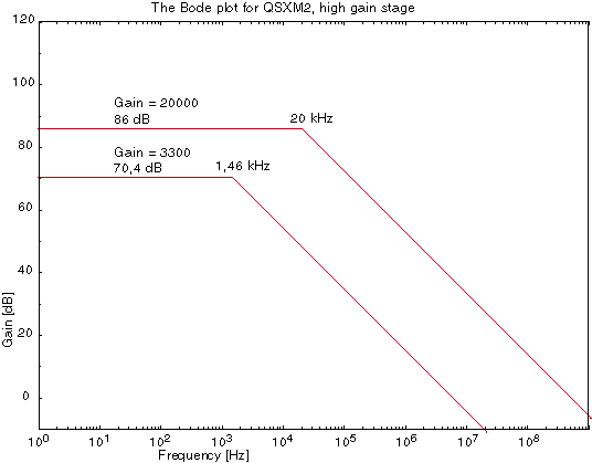
The cascode stage is a very useful combination of two transistors. The benefits are two, lower distortion and dramatically extended frequency response. T27 and T29 is one of the cascodes. The gain is 20000(!) and the bandwidth 20 kHz. Maybe it's not that interesting to know why the stage gets faster, but it's true. But why does the distortion decrease?
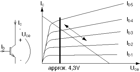
The bipolar transistor is a current driven device. You are only interested in input (base) current and output (collector) current. The picture above shows that the current gain is dependent of the applied voltage on the collector. If i.e. Hfe is 300 at 1 mA and 25V, it gets 350 at 35 volts. The current gain isn't a constant parameter. It changes also if you change the base current. 10 uA base current generates 1 mA, 20 uA, 2,2 mA, 30 3,6 mA. The fact that the current gain isn't constant generates harmonic distortion. But the greatest "defect" is the sensitivity for varying collector voltages.
If you take out the output signal at the collector with a help from a collector resistor, you'll get a signal that moves along the load line, see above. The graphical way of showing it is that the lines for Ib1, Ib2 etc. gets more separated at higher collector voltages, at the right. This is a sign that the current gain is higher than at the left (low collector voltages). Parallel, but maybe inclining, lines is a sign of constant current gain.
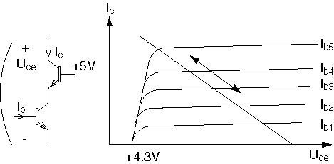
If you try to keep the collector voltage constant and in some way try to use the collector current you get interesting results. The "magical" load is the input of a base grounded stage. The base is at a constant potential with respect to signal ground. The input impedance of a such stage is very low, 25 ohms at 1 mA, 2,5 ohms at 10 mA. The base grounded stage isolates the first transistor from collector voltages variations.
The results of this are:
- Elimination of the Miller effect and therefore increases (extends) the frequency response dramatically
- Reduction of distortion
- Creates a super transistor with high gain, high voltage and high speed and also high power in some circumstances.
Advantage to use cascodes in an input stage:
- Faster input stage and therefore easier to feedback and to get a stable combination. The input stage should be as fast as possible.
- Possibility top use low voltage and low noise transistors and high supply voltage, especially important in power amplifiers.
Advantage to use cascodes in a high gain stage:
- Possibility top use low voltage and fast transistors together with high voltage ones and achieve high gain at high voltage swings.
- Low distortion
- Faster stage (sometimes an advantage)
Explanations of the specific design, the pre amp.
Please download all the schematic pages and print them out. It's much easier to understand what I'm talking about if you look at the circuits at the same time. I will only talk about the left channel and the upper half. The design is symmetrical and the two channels are identical.
The input filter
It's very important to tune the input impedance in order to achieve flat frequency response. If you choose to use the input bias servo (see page 7) the input impedance will be 270 kohms (R97) and if you choose not it's several megaohms (you can ignore it).
R1 together with R97 creates 47 kohms needed for most MM pickups and R3 is for MC pickups.
R2 together with C2 is an EMI-filter. In order to achieve the lowest noise possible R2 should be 0 ohm if you don't have any RF interference. If you have some trouble start first with:
- a wire with ferrite beads
- a bigger ferrite inductor with one or few windings
- an inductor 100µH to start with
- a resistor, 10-100 ohms (avoid due to increased noise, especially in MC mode)
Correct pickup load
It's important especially for MM-pickups to have correct load. Too little capacitance creates a sharp resonance peak at 8-20 kHz which can cause a sharp treble sound. The resistance is determined by R1 (MM), R2 (MC) and R97. The right capacitance is also important, especially for MM-pickups. 100-500 pF is normal values. Consult the pickup manufacturer for the right value. MC-pickup demands much bigger capacitance C2. I have chosen 10 nF. Normally MC don't need any input capacitor but to be sure, consult the datasheet of the pickup. With jumper J1 you can in an easy way change load. The best solution is to solder the jumper pins (and exclude the jumper itself) but I think the contact in the jumper is quite good.
The differential (input) stage
Current source (for the negative half) for the stage is DZ1 sets a 6.8 V voltage, feed through a LP-filter (R7, C3, C5) with reduces noise from zener and power supply and makes the amp start up nice when the power is switched on. The voltage drop across R7 is approx. 0.4-0.5 V. This makes a voltage across R9 of 5.65V. The current is therefor 1.45 mA divided in four equal parts through R17, R19, R21, R23 feeding the differential transistors (T5-T23, T7-T21, T9-T19, T11-T17) which can be separate components or monolithic and matched pairs.
T13 and T15 forms a cascode together with the lower transistor pairs. This type of stage extends the frequency response by a factor of at least 10. The distortion is also reduced. T3 creates a constant current and a constant voltage across R13 related to ground. The voltage is approx. 4.6 V. T13 and T15 are biased via R15 and smoothed by C11 and C15.
In order to get low noise the input transistors should not have any emitter resistor (no resistance between its emitters i.e. T5 emitter to T23 emitter).
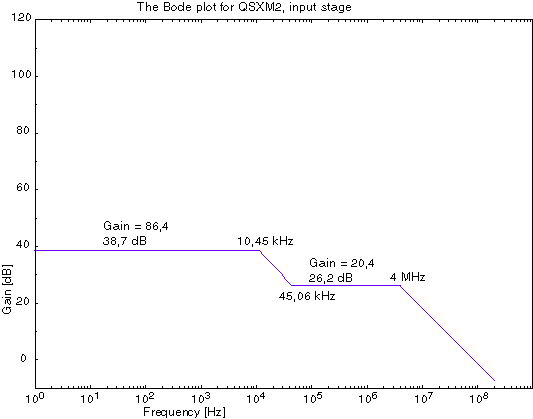
The gain is (at room temperature 25°C) A = Ic * Rc* 0.040 * 1/2= 1.45*10-3 * (2200 + 680) * 0.040 *1/2 = 83 = 38 dB.
You can see that the frequency response is not flat. This is because I wanted to optimize the noise performance. Maybe there is some combination which is better but I haven't investigated that. You can probably use a little bit less gain in both the input stage and the high gain stage. There is no problem to lower the gain just in increasing it. When you increase the gain sooner or later you will get oscillations.
Noise improvements
The noise performance is the best at 100-300 µA and MM-pickup with BC550/560 transistors. 1 mA or more is the best for MC-pickup. If you use MAT02/03 the optimum current is approx. 1-5 mA. If you use MM-pickup it's also recommended to have 1 mA at least. If you choose to use MAT02/03 I recommend 1 mA through each transistor. Don't forget to lower the value of R25 and R31 and increase C7.
If you use transistors in parallel the noise is lowered by a factor of square root of 8 (= 2.8 = 9 dB).
Noise improvements with extra pairs:
| No of pairs | Factor square of | Factor | dB |
| 1 | 2 | 1.41 | 3 |
| 2 | 4 | 2 | 6 |
| 3 | 6 | 2.4 | 7.8 |
| 4 | 8 | 2.8 | 9 |
| 5 | 10 | 3.2 | 10 |
| 6 | 12 | 3.5 | 10.8 |
| 7 | 14 | 3.7 | 11.4 |
| 8 | 16 | 4 | 12 |
| 9 | 18 | 4.2 | 12.6 |
| 10 | 20 | 4.5 | 13 |
| 11 | 22 | 4.7 | 13.4 |
| 12 | 24 | 4.9 | 13.8 |
| 13 | 26 | 5.1 | 14.1 |
| 14 | 28 | 5.3 | 14.5 |
| 15 | 30 | 5.5 | 14.8 |
As you can see, the improvements gets smaller and smaller the more pairs you use. More than 4 pairs are not very wise. It's better to choose other components with lower noise.
The emitter follower after input stage and cascode
The emitter follower T25 decreases the effect of the load from the high gain stage T27 and T29. The result is mainly extended frequency response of the first stage. The second result is lower distortion. The main advantage of the emitter follower is increased phase margin and therefore better stability when the whole amp is feedbacked. The odds not to have oscillations increases.
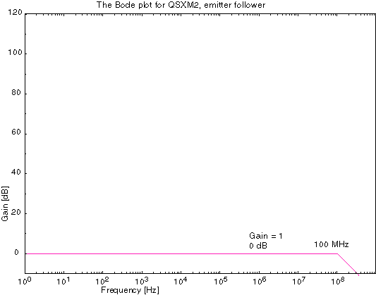
The frequency response of the emitter follower is very high and also a little bit tricky to measure it. The value above is a guess.
The high gain stage
The important high gain stage is formed by T27 and T29. A minor local feedback is created by R35. The total gain is quite extreme, approx. 20000 times! The gain is lowered further with R37. The result is gain determined by R35/R37 = 3300 (70 dB). C17 creates a dominant pole in order to get a stable amplifier when feedbacked. The gain is very easy to adjust, just change the relationship between the mentioned resistance's. If the pre amp always shall work in MC-mode, it's possible the lower the capacitance's in order to get a faster stage and lower the distortion. An easy way to test how small the capacitance can be, apply square wave and trim for a perfect step response. The value of C17 is a compromise in order to use MM and MC pickups without any trimming, just changing a jumper.
The fast output stage
I have chosen cheap but fast small signal transistors to get a very fast output stage. Since the rated power is rather small and load is rather heavy (the feedback resistors) it's necessary to use three pairs. The feedback resistors have to have a low resistance in order to get the lowest noise possible.
The reason why I have a LED as bias voltage generator is, easy to get a stable bias current and low values of the emitter resistance's and therefor a low output impedance. Low impedance is important when driving low impedance loads in order to get low distortion. Oh, I forgot, LED looks cool! You don't have use red LED but if you change colour notice that the current will increase due to higher forward voltage. But this is not a problem, just adjust the emitter resistors (R43-R47, R82, R83) to a little bit higher value.
Test point
TP1 is a test point in order to be able to measure the pre amps characteristics in an easy way. The printed circuit board has groundplane and it's very easy to short down to ground when measuring and by that damaging the amp.
DC-servo
It's virtual impossible to get good DC-performance without some kind of servo (based on good opamps). The servo has some difficulties to be connected conventionally to the junction of the inverting input (base of T23 etc.) because of the low resistor values. The servo will consume a great deal of power but otherwise it's not a problem.
I have chosen to inject current inside the amp instead. Through R27, R29 a small current is either injected or drained. C9 makes sure that no audio signal goes into the servo and also that the servo not introduces any noise. The opamp IC1 should be a decent type with good DC-performance, slow and with low noise. The speed of the opamp should be not more than 1 V/µs. The opamp works as a non-inverting integrator. You should always have symmetrical component values in order to get a true integrator and also to get low offset caused by input offset currents of the opamp.
Input bias servo
Because the input stage has noticeable input current, an offset voltage is always present. If ultra low noise transistors are used, this servo is very important because of the high base current from the negative half. The PNP types of this transistor type has rather low current gain and the NPN-type rather high. This causes an unbalance in base currents. IC5 works a normal inverting integrator which strives to keep the output of the opamp at zero volts. The servo speed is very dependent of the pickup resistance. MC pickup creates a time constant of minutes and MM pickup creates time constant around one minute.
Feedback
The total gain (all of the separate diagrams combined) shown in this picture.
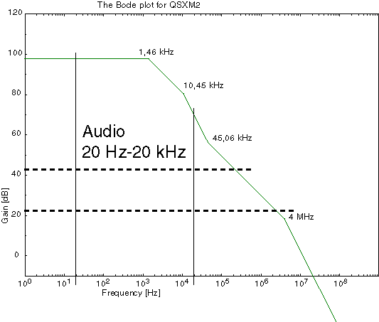
Long time ago when I made the original of the diagram, I made a mistake. I made the open-loop gain too high (not knowing). My goal was 100 dB gain but it became 108 dB. In real life the emitter follower is a substantial load together with the feedback network. Therefore the gain is a little bit lower.
Attention: Don't connect or disconnect the pickup when the amp is turned on! The servo creates a large spike which can damage your power amp, speakers, headphone!
The servo is slow in order to be able to work in background and not disturb the pickup signal in any audible way. My special kind of circuit attenuates the opamps inherent noise and to be sure it's a really low noise servo I have chosen an extreme chopper stabilized opamp. The special circuit makes the servo slow. With MC-pickup we talk about a minute or more to settle. With MM-pickup it's a couple seconds in settling time.
SMD types, alternative transistors
Long time ago (in 1986) when I first designed this amp it was very easy to get good hole mounted types of transistors but now it can be quite hard to get good transistors with high gain. It's rather easy though to get good surface mounted types. Therefore I have made room for SMD types in every transistor position. I have also included the possibility to use cheap transistor pairs (very small devices) and for matched ultra low noise matched pairs. SMD transistors aren't so hard to solder by hand but BC847BS/BC857BS are not suitable for newbeginners, only if you are VERY handy with the soldering iron.
The RIAA-amp
Most of the design is the same for the correction amp as for the preamp. The difference is only one transistor pair in the input stage, a single output stage and connected as an inverting amplifier. This amp is not so critical as the ultra low noise preamp. Here we don't need neither low noise performance or high current output. R84 serves as a simple short circuit protection and together with C53 it forms a LP-filter (EMI-filter). The cut frequency is 459 kHz. I think it's wise to have some protection against RF-interference. This filter can be omitted but leave the resistor R84 so you have short circuit protection. The output stage can drive a rather long cable with good results. I think at least 10 m or 30 ft is no problem.
This amp is a little bit slower than the pre amp because of the need to be stable at gain of 1 (no gain). C41 has a larger value than C17.
The RIAA-correction filter
The RIAA-curve and the circuit is explained here.
The capacitors for the RIAA-network should be high performing and with tolerance of less than 5%, preferable 2.5%. If you can't get hold of precision caps it's OK to measure up 5 or 10% caps. I think both polycarbonate and polyester will work rather well but I recommend polypropulene.
The pcb layout
The component print
The picture shows the component print of the PCB. Of course you can't use it for anything except for an overview. Please download the pdf-file instead if you want to see the details.
The printed circuit board is made for two channels. It's possible to do this pcb by yourself. Just make the layout as the schematics. As you can see I have done it. The pcb have groundplane on the upper side (not shown in pictures) which is essential in order to get good results. I haven't made it easy for switching pickup. I gather you will use only one type and also trim for this type.
The solder side
The picture shows the solder side of the PCB. Of course you can't use it for anything except for an overview. Please download the pdf-file instead if you want to see the details.
Almost everyone of the traces are on the solder side. The groundplane is very covering, only a few traces on the component side.
The component side
The picture shows the component side of the PCB. Of course you can't use it for anything except for an overview. Please download the pdf-file instead if you want to see the details.
Almost everyone of the traces are on the solder side as you can see. The groundplane is very covering, only a few traces on this side.
The component side of the real pcb
The picture shows the component side of the PCB, the real one.
The solder side of the real pcb
The picture shows the solder side of the PCB, the real one.
As you can see the pcb exists in the real world. The first prototype of the new pcb is built. I'm quite pleased. If you are interested in building my amp with the amazing performance , don't hesitate to get in contact with me. Since I wrote this for the first time many new QSXM2 amps have seen the day of light.
The extremely small BC847BS and BC857BS
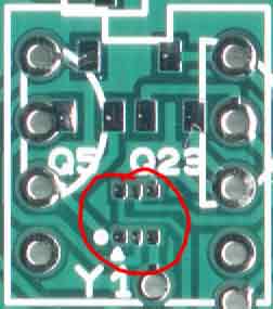
I have equipped the pcb with option for BC847BS/857BS matched pair. This device is very small but it's not impossible solder by hand. See picture below. You can also see the footprints for SMD devices, above Q23.
A SOT363 adapter
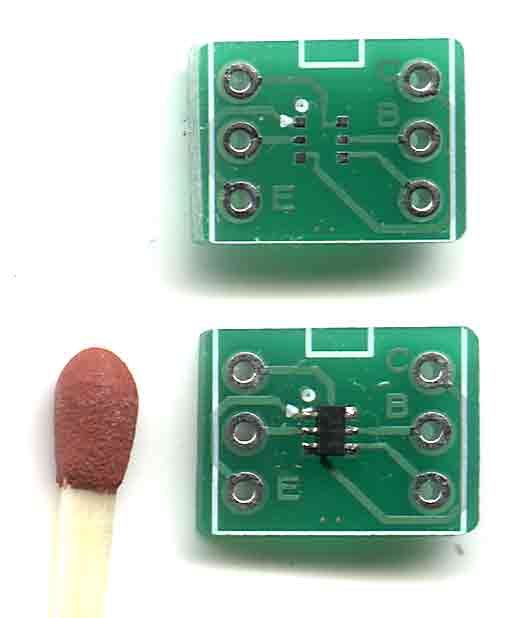
This tiny device is two matched ordinary BC847 (=BC547) in one package and they are also isolated from each other.....and....they are cheap! I have only made 5 pieces of this pcb but do I see some interest I will manufacture this little adapter. It fits an ordinary DIL-6 socket and can be a cheap replacement for MAT02 or 03.
Recommended power supply
SSR03 is a very low noise stabilized power supply. Of course I recommend it (I designed it for this purpose!) but any low noise power supply will do but you must consider the rather low power supply rejection ratio (PSRR) the QSXM2 has. Therefore it can't reject noise as much as an opamp based amp can.
The best power supply unit consists of two QSXPS pcb's and two transformers. This solution costs much but is undoubtly the best. I think also that a 7815/7915 or LM317/337 based power supply can be equally good if lot's of smoothing caps are used. You can check QSXM3 and the built-in power supply for inspiration.
Component choices
I have nothing against "audiophilic" components but this design requires normal standard good performing industrial parts as a good start and will work correctly if the recommend parts are used. Feel free to change the parts you like but you must have control over the important electrical parameters of each part. I'm aware of that certain parts "feels" right and as long as they fit, use them!
I think that some of the "audiophilic" parts are just plain froud. They have absolutely no documented "audiophilic" features what so ever. Same parts are only known but rumours over the internet and magazines. In many cases no double blind tests have taken place.
Build directions
Before you build, take a look at possible component selections and trimming. It doesn't harm to skip this but maybe it feels better in knowing to have a more symmetrical amp than you would have otherwise.
Have you noticed my method of naming the components? The reason why I did this is to limit the length och the parts name. A few components have number above one hundred. It's more difficult to get a clear marking on the pcb if the parts name is too long.
Left channel, right channel
R1 = E1 (resistors)
C1 = G1 (capacitors)
T1 = V1 (transistors)
Q1 = N1 (SMD transistors)
Y1 = U1 (SMD matched transistors)
Above is valid for all components except for (my mistake when I made the pcb):
R27 = E29
R29 = E31
R31 = E27
The amp can be build in two different ways: The big bang method or the cautious method. It's nothing wrong with the big bang method if you are experienced and/or skilled.
The big bang method
Solder in everything and then apply voltage. If you are thorough, the amp works.
If you want to trim anything read this first.
Recommended solder order (just for practical reasons). Start with low components and then take parts with bigger height. If you wait with the transistors you will have rather high caps as distances. This will make it much easier to solder in the transistors nice and straight.
- Transistors (SMD)
- Resistors
- Zeners
- Capacitors, plastic
- Capacitors, electrolytic
- Transistors (hole mounted)
- Connectors
- Opamps, but wait until you have made the first test.
Error reports
Mixed up naming left, right channel but the schematic is correct.
R27 = E29
R29 = E31
R31 = E27
Esthetic error in the pcb
G56 and G57 have changed physical positions. G56, 57, 58 are all parallel connected. If you want it to "look right", let G56 and G57 change positions.
Z11 has the lost the last "1" because the pcb manufacturer removes all print in the pads.
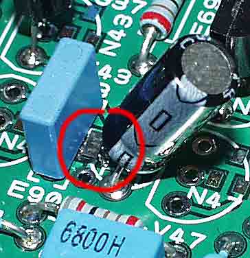
Error in the pcb
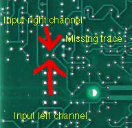
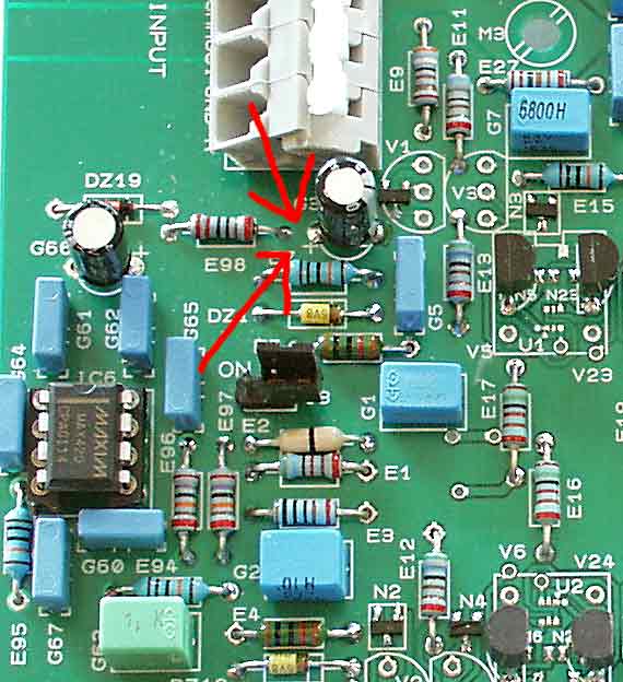
This error is fixed in the second production batch. E98 has a missing trace towards +15 volts. Correct this with a short wire (use the leg of E98!) on the solder side. See pictures below.
Click on the picture to get a larger view.
The cautious method (recommended for most people)
If you want to trim anything read the section about trimming first.
Solder in all passive parts. Then solder some active parts and then test the function. If it's OK solder in more parts. This method is quite good if you have bought my rather expensive pcb's and want to have a nice looking result.
Recommended solder order
Recommended solder order (just for practical reasons). Start with low components and then take parts with bigger height.
- Resistors
- Zeners, match (if you want to) each pair DZ1 and DZ2, DZ5 and DZ6, DZ11 and DZ12, DZ15 and DZ16. The zeners should have the same value pairwise. Match them with same current as they will have in the circuit. Take 10 kohms in series and 15 or 18 volt.
- Capacitors, plastic
- Capacitors, electrolytic
- Connectors
- Transistors (hole mounted and/or SMD), see text below. Hole mounted transistors should have short legs, 5 mm is max. It's recommended to have a compact design. The transistors are more protected and the RF-rejection is improved (shorter antennas).
- Opamps, but wait until you have made the first test.
Check one channel
Check one channel at the time. Start with the left channel. The building advice is for the left channel but the same goes for the right.
Solder first everything except for transistors. You can also solder all the components which are connected to the transistors in mind but it's no danger to solder all passive components first. Maybe it's easier to get an overview if not all passive components are in place.
Start to check the preamp, then the RIAA-amp, one channel at the time. Note that you can apply voltage to one channel at the time.
- The transistors for the input stage. Start with T1-T26. Place a jumper at J1. The input will be more or less shorted. Apply voltage and measure the DC-voltages but bare in mind that the stage has a certain unbalance because it has no feedback.
- After that take T27-T36. Place a jumper at J1. The input will be more or less shorted. Apply voltage again and measure the DC-voltages. Now the amp has feedback but it should still have a minor unbalance, DC-voltage at the output. Up to 1 V at the output (TP1) can be expected.
- Check the range of the DC-servo. Apply 15V at pin 6 of IC1, and of course, no opamp in place. You should get a negative voltage at the output. Apply -15V at pin 6 of IC1. You should get a positive voltage at the output. If you don't get negative and positive output voltage you must lower the value R27, R28, R29 and R30. The DC-servo won't work otherwise. You must have symmetrical values of these resistors. R27 and R28 can have one value and R29 and R30 an other. Change the value in small steps. I think 68 kohms will cover all situations but it's less interfering with high values.
- Insert the IC1 opamp. Apply voltage. The output offset should be the same value as the opamp itself. < 0.5 mV is good but you set the limit for what it's good. I recommend that you don't use IC sockets and if you still want use high quality with "tulip" contact. I have used sockets only for development. Don't use them!
- Insert the IC5, chopper stabilized opamp for the input bias current servo amp. You can also use a slow low noise precision opamp but remember to remove the zeroing caps, C61, C62. If you use a normal opamp you don't need the zeners either, DZ9, DZ10.
- Check the servo. Apply J1. Apply voltage and have a voltmeter at the output, TP1. Remove the jumper and observe the output transient. After a while the output should be zero. This will take some time. If you test with a MC pickup (or a low resistance it will take minutes. The servo is necessary with super low noise transistors both with MM and MC pickup and with MM pickup with BCxxx transistors. With BCxxx and MC it's not a problem with base currents.
The whole pcb
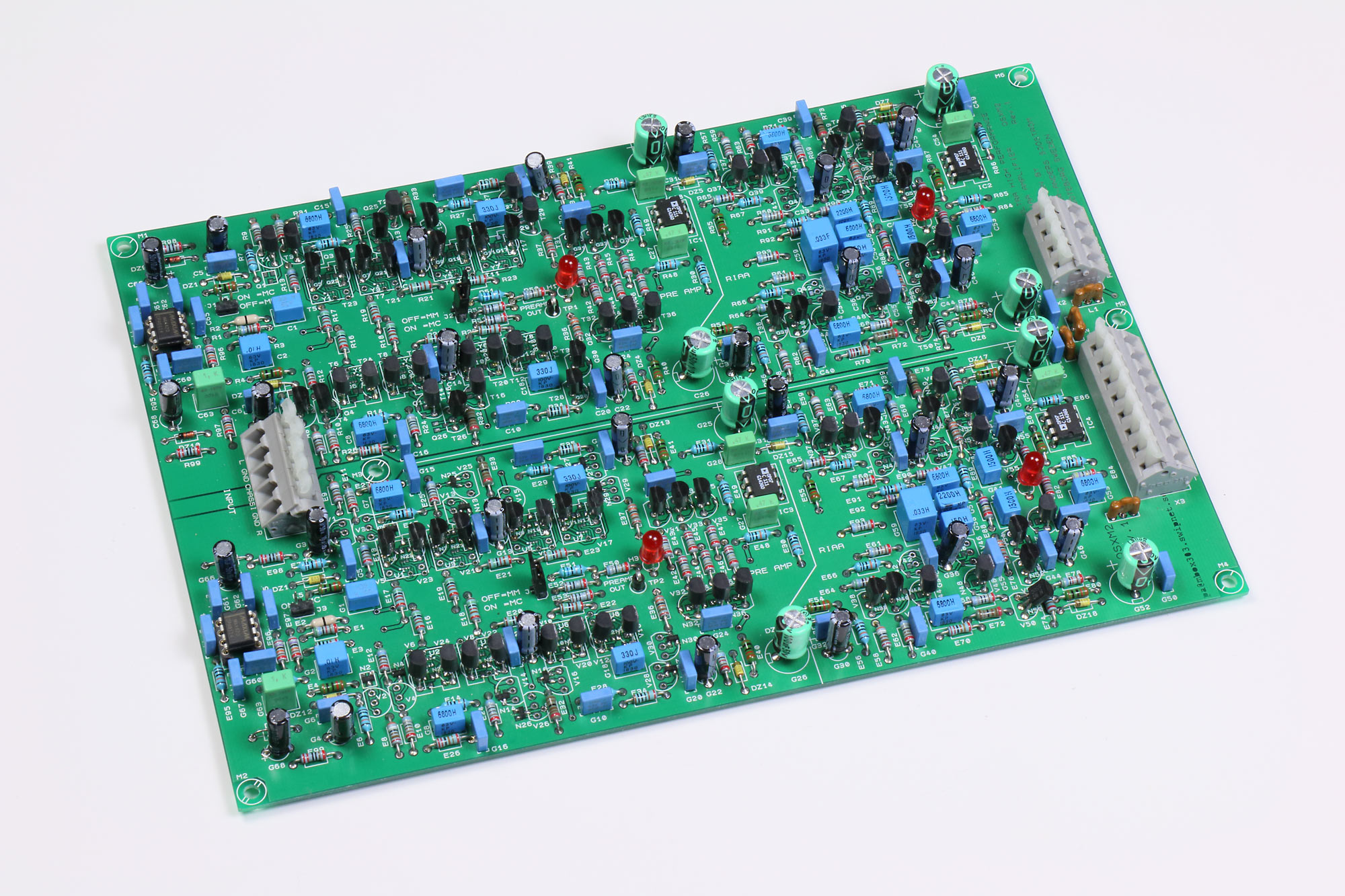
Click on the picture to get a larger view.
The complete phono amp with all components soldered in. The right channel (lower half of the pcb) has some SMD transistors. This is only for the picture taking.
The RIAA amp
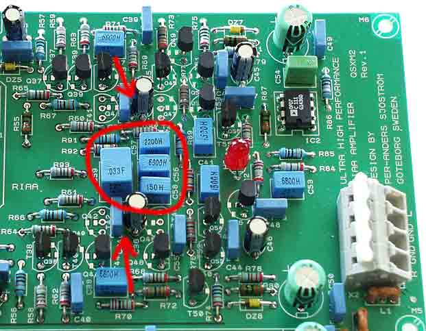
Click on the picture to get a larger view.
Detail of the RIAA amp. The marked capacitors are the RIAA correction network. It's important that those caps have low tolerance, or measured.
SOT-23, surface mounted transistor
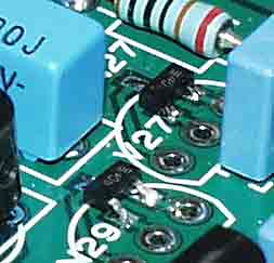
Click on the picture to get a larger view.
Here is a detail of the SMD transistors. Every transistor can be SMD type if you want or can't get good hole mounted types.
SOT-23 and TO-92, surface mounted and hole mounted transistors
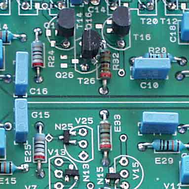
Click on the picture to get a larger view.
Here is an another detail of the SMD transistors.
SOT-363 BC847BS, BC857BS, surface mounted matched transistor pair
Click on the picture to get a larger view.
Here is an another detail of the SMD matched transistors pairs with are in the input stages. They are not easy to solder because they are so tiny. The are quite good though if you compare the price. Beware of that this type has no noise parameters. They can be noisier than other types which has specified noise figures. If you plan to use MM pickup only noise figure isn't so important (compared to MC pickup). With 8 pairs the noise will always be lower than needed in MM mode.
Click on the picture to get a larger view.
This picture shows how small BC847BS and BC857BS really are.
Trimming, tweaks
I haven't got any suggestions for real tweaks. I'm not a big fan of this kind of voodoo but if you have, please feel free to email them to me. Maybe they can be useful for others.
Trimming
If you change C17 and C18 ( pre amp) and C41 and C42 (correction amp) you can trim the slew rate and by that also sonic properties. It's wise to have the speed adjusted to perfect step response. It's not recommended to have the amp too fast with overshoots.
Preamp with BC550/560, MM-mode
14V/1,0µs (14 V/µs), 330 pF, perfect step
14V/0,6µs (23 V/µs), 220 pF, perfect step
14V/0,5µs (28 V/µs), 150 pF, perfect step
14V/0,25µs (56 V/µs), 100 pF, minor ringing
Preamp with BC550/560, MC-mode
14V/1,0µs (14 V/µs), 220 pF, perfect step
14V/0,25µs (56 V/µs), 100 pF, perfect step
14V/50ns (280 V/µs), 0 pF, perfect step
In MC-mode the amp has no slew rate limiting and therefore a nice clean step response.
DC-voltages in an amp with feedback
Use a multimeter 10 Mohms inimpedance. All values are voltage across the component.
+-15.0 V supply voltage were used.
Pre amp, Left channel, MM-mode, BC550C, BC560C in all positions, OP07 as DC-servo, no input bias servo, input not shorted.
DZ1, 6,96V
DZ2, 6,96V
DZ3, 7,08V
DZ4, 7,09V
R1, -9,5mV, current into the amp. NPN-transistors have slightly lower Hfe than PNP. Total resistance is 47 kohms, 0,2uA, input bias current.
R6, 491mV, 4,91uA
R7, 438mV, 4,38uA
R8, 5,85V, 1,500mA
R9, 5,88V, 1,508mA
R10, 5,86V, 862uA
R11, 5,90V, 868uA
R12, 4,80V, 857uA
R13, 4,83V, 862uA
R14, 200mV, 2,00uA
R15, 299mV, 2,99uA
R16, 5,64V, 376uA
R17, 5,61V, 374uA
R18, 5,64V, 376uA
R19, 5,61V, 374uA
R20, 5,64V, 376uA
R21, 5,61V, 374uA
R22, 5,64V, 376uA
R23, 5,61V, 374uA
R24, 508mV, 747uA
R25, 518mV, 762uA
R26, 1,65V, 750uA
R27, 9,15V, 91,5uA
R28, 3,65V, 36,5uA
R29, 9,12V, 91,2uA
R30, 3,62V, 36,2uA
R31, 1,68V, 764uA
R32, 1,56V, 1,418mA, (1,1kohms)
R33, 1,58V, 1,436mA, (1,1kohms)
R34, 926mV, 9,26mA
R35, 926mV, 9,26mA
R38, 834mV, 14,9uA
R39, 855mV, 15,3uA
R42, 325mV, 14,8mA
R43, 319mV, 14,5mA
R44, 321mV, 14,6mA
R45, 319mV, 14,5mA
R46, 316mV, 14,4mA
R47, 323mV, 14,7mA
C3, 6,46V, Vbe, T1 580mV
C4, 6,40V, Vbe, T2 550mV
C19, 5,28V
C20, 5,30V
H1, 1,82V
PREAMP_OUT_L, <+-0,2mV, changing with temperature fluctuations and air movements
DC-ADJUST_L, -5,66V, can go between +12-13V to -(12-13)V depending of balance.
Pre amp, Right channel, MM-mode, BC850C, BC860C in all positions, OP07 as DC-servo, no input bias servo, input not shorted.
DZ11, 7,14V
DZ12, 7,11V
DZ13, 7,05V
DZ14, 7,18V
E1, -3,1mV, current into the amp. NPN-transistors have slighty lower Hfe than PNP. Total resistance is 47 kohms, 66nA, input bias current.
E6, 479mV, 4,79uA
E7, 513mV, 5,13uA
E8, 5,98V, 1,533mA
E9, 5,98V, 1,533mA
E10, 6,03V, 887uA
E11, 6,00V, 882uA
E12, 4,90V, 875uA
E13, 4,90V, 875uA
E14, 255mV, 2,55uA
E15, 302mV, 3,02uA
E16, 5,73V, 382uA
E17, 5,72V, 381uA
E18, 5,73V, 382uA
E19, 5,72V, 381uA
E20, 5,74V, 382uA
E21, 5,72V, 381uA
E22, 5,74V, 382uA
E23, 5,71V, 381uA
E24, 470mV, 691uA
E25, 469mV, 690uA
E26, 1,527V, 694uA
E27, 1,527V, 694uA
E28, ----
E29, ----
E30, ----
E31, ----
E32, 1,388V, 1,262mA, (1,1kohms)
E33, 1,394V, 1,267mA, (1,1kohms)
E34, 748mV, 7,48mA
E35, 752mV, 7,52mA
E38, 666mV, 11,89uA
E39, 727mV, 12,98uA
E42, 373mV, 16,95mA
E43, 373mV, 16,95mA
E44, 381mV, 17,32mA
E45, 367mV, 16,68mA
E46, 383mV, 17,41mA
E47, 368mV, 16,73mA
G3, 6,56V, Vbe, V1 580mV
C4, 6,56V, Vbe, V2 580mV
C19, 5,54V
C20, 5,74V
H3, 1,80V
PREAMP_OUT_R, see below!
DC-ADJUST_R at +15 V gives -0,177V at output, -15 V gives -0,0185V. Can go between +12-13V to -(12-13)V depending of balance. This particular amp needs some adjustment in the offset adjusting range ,
Comments about the measurements
You can see a difference between hole mounted transistors and surface mounted ones. Places where the dissipated power is low there are no major differencies but in the output stage the transistors get much hotter due to less effective cooling. Otherwise the performance is more or less identical.
Correction (RIAA) amp, Left channel, BC550C, BC560C in all positions except for the input stage BC847BS, OP07 as DC-servo, input shorted.
DZ5, 6,99V
DZ6, 6,98V
DZ7, 7,03V
DZ8, 6,60V
R93, 0,92mV, current into the amp. NPN-transistors have slighty lower Hfe than PNP. Total resistance is 680 ohms, 1,35uA, input bias current.
R56, 1,14V, 11,4uA
R57, 1,10V, 11,0uA
R58, 5,24V, 1,344mA
R59, 5,25V, 1,346mA
R60, 9,71V, 1,428mA
R61, 9,10,V 1,338mA
R62, 5,25V, 772uA
R63, 5,28V, 776uA
R64, 4,28V, 764uA
R65, 4,33V, 773uA
R66, 183mV, 1,83uA
R67, 209mV, 2,09uA
R68, 446mV, 656uA
R69, 451mV, 663uA
R70, 1,45V, 659uA
R71, 1,47V, 668uA
R72, 1,31V, 1,191mA (1,1kohms)
R73, 1,32V, 1,200mA (1,1kohms)
R74, 667mV, 6,67mA
R75, 665mV, 6,65mA
R78, 629mV, 11,23uA
R79, 687mV, 12,22uA
R82, 338mV, 15,36mA
R83, 337mV, 15,32mA
R89, 0,96mV, from the inverting input,
C30, 5,84, Vbe T38 600mV
C43, 5,64V
C44, 5,27V
H2, 1,89V
+15 V at pin 6, IC2 (without an opamp) gives +81mV at output, -15 V gives -79mV. Can go between +12-13V to -(12-13)V depending of balance.
Listening experience
|
|
| Click on the picture to get a larger view.
The front view of the QSX Amplifier. |
Click on the picture to get a larger view.
The printed circuit board of the QSX Amplifier |
Why is it so important with the phono amplifier in order to get good sound quality?
A real difference
I thought, honestly speaking (back in 1986), that I couldn't hear any real difference between different kinds of phono amps. Boy, was I wrong! The difference can be small but noticeable to huge! I'm not joking here. A good vinyl, played with a good turntable and good RIAA correction amp can sound really, really good, but I don't say that vinyl is better than digital sound. Because we have a huge vinyl collection we don't have to play the with bad gear. The vinyls are worth to be played with good hifi stuff.
A fragile link
Today the amplifier and the CD are the strongest links in the hifi chain. When the vinyl was popular there were very often deficienies in the phono amp department and surprisingly often nowadays if you buy a 100-300 dollar unit!
Cheap junk
Nowadays you can buy rather cheap separate amps with very poor sound quality (of course there are better ones too). I made 'reverse engineering' of one amp in the price region of 50 dollars. I was horrified, to be short! Junk! I have also looked at more expensive ones and I'm not impressed.
What makes the phono amp good?
The main design problem is to make an amplifier with an output stage which can deliver rather much current into a highly capacitive load, the RIAA correction filter. The correction filter may have an impedance of 300 ohms purely capacitive which means that the output stage must be able to deliver 10 - 20 mA with a phase angle of +90°. This is a difficult task to do together with low distortion and a stable signal shape. Many amps can't deliver square wave into a capacitive load without overshoots. The other considerations are low noise and low distortion, not so hard to achieve.
One forgotten thing is the input impedance. If you have too low input capacitance (for your the chosen pickup) you get very often a very sharp resonance peak at 10-20 kHz. This is sometimes a positive effect to a tired old amp with an equally tired cassette deck but is a bad thing in a modern stereo and good loudspeakers. Especially MM-pickups are sensitive. My Ortofon FF15 needs around 400 pF in order to sound good. MC-pickups are not that sensitive but they still need correct load.
How does it sound when the output capability is low?
The sound is without life, like seeing through dirty glasses, like an old Dolby-C recording. You can't put finger on what's wrong. The high tones are especially effected. If you can compare with a better amp, you are surprised how big the difference can be! The clicks and noise sounds also different. A slow (or bad) amp can't handle click equally well as a high performance amp. With a good amp you will get much more listening pleasure, sounds nicer, the clicks aren't that irritating
How good does vinyl sound really?
We (me and my friend) amused ourselves one evening with comparing CD and the same album on vinyl. Test albums were (don't forget it was 1986): Dire Straits, Brothers in arms, Benny Andersson & Björn Ulvæus (ABBA), Chess, Roger Waters, Pros and cons of hitch hiking and David Bowie, Let's dance. These albums were recorded with digital technology. With normal listening levels (quite high actually) there were only minor differences between CD and vinyl. But when the volume was very high, of course, you could hear noise, clicks and rumble from the vinyls. You must play at quite high volume in order to determine which sound source is CD and vinyl.
With this I want to say that my phono amp can measure itself with very expensive amps if you use it for MM-pickups. The amp in MC-mode is also high performing but you can make some enhancements if you replace the transistors in the input stage.
The original design used only low price transistors but my brand new professional pcb has been equipped with the possibility to use ultra low noise matched transistor pairs.
How does it sound nowadays?
I have now listened to the remake of the amp. I'm very pleased to be short. It's was so exciting to apply voltage for the first time and connect my headphones directly to the output of the amp. The first albums were Anabel Lamb, the first and second and Donna Summer, "Living in America". I notice that I have forgotten how good vinyl can sound. It was now some time since I listened to vinyl with critical ears. It's fun!
Technical data
The preamp is connected for MM-pickup
| Frequency response: | 0 Hz - 4,2 MHz, -3 dB |
| Frequency response with DC-servo: | 0,4 Hz - 4,2 MHz, -3 dB |
| Power bandwidth at 10 Vrms, 68 ohms: | 0,4 Hz - 270 kHz, -3 dB |
| Equivalent input noise: | 220 nV |
| Equivalent input noise, with perfect balance: | 160 nV (25 nV with super low noise transistors) |
| Signal to noise ratio: | 93 dB |
| Signal to noise ratio, with perfect balance: | 96 dB (109 dB with super low noise transistors) |
| Dynamic headroom: | 131 dB |
| Dynamic headroom, with perfect balance: | 134 dB (150 dB with super low noise transistors) |
| Distortion: | < 0,001 % |
| Slew rate: | 19 V/us |
| Step response: | Perfect without overshoot |
| Gain: | 13 (22 dB) |
| Input impedance: | 47 kohms// 470 pF (0-270 kohms//20 pF and up, limited only by physical dimensions , user selectable) |
| Output impedance: | 800 micro ohms |
| Output current: | 300 mA |
| Gain bandwidth product: | 750 MHz |
| The amp uncompensated | |
| Frequency response: | 0 Hz - 13 MHz, -3 dB |
| Power bandwidth at 10 Vrms, 68 ohms: | 0,4 Hz - 440 kHz, -3 dB |
| Gain bandwidth product: | 12 GHz |
| Slew rate: | 31 V/us |
The preamp is connected for MC-pickup
| Frequency response: | 0 Hz - 270 kHz, -3 dB |
| Frequency response with DC-servo: | 0,4 Hz - 270 kHz, -3 dB |
| Power bandwidth at 10Vrms, 68 ohms: | 0,4 Hz - 270 kHz, -3 dB |
| Equivalent input noise: | 220 nV |
| Equivalent input noise, with perfect balance: | 160 nV (25 nV with super low noise transistors) |
| Signal to noise ratio: | 71-76 dB |
| Signal to noise ratio, with perfect balance: | 74-80 dB (90-96 dB) |
| Dynamic headroom: | 111 dB |
| Dynamic headroom, with perfect balance: | 114 dB (130 dB) |
| Distortion: | < 0,001 % |
| Slew rate: | 14 V/us |
| Step response: | Perfect without overshoot |
| Gain: | 137 (43 dB) |
| Input impedance: | 100 ohms// 10 nF (0-270 kohms//20 pF and up, limited only by physical dimensions, user selectable) |
| Output impedance: | 13 mohms |
| Output current: | 300 mA |
| Gain bandwidth product: | 750 MHz |
| The amp uncompensated | |
| Frequency response: | 0 Hz - 440 kHz, -3 dB |
| Power bandwidth at 10Vrms, 68 ohms: | 0,4 Hz - 440 kHz, -3 dB |
| Gain bandwidth product: | 12 GHz |
| Slew rate: | 31 V/us |
The correction (RIAA) amp
| Frequency response without correction network: | 0 Hz - 6 MHz, -3 dB |
| Frequency response without correction network with DC-servo: | 0,4 Hz - 6 MHz, -3 dB |
| Power bandwidth at 10 Vrms, 68 ohms: | 0,4 Hz - 51 kHz, -3 dB |
| Equivalent input noise: | 700 nV |
| Distortion: | < 0,001 % |
| Slew rate: | 3,5 V/us |
| Step response: | Perfect without overshoot |
| Gain: | 16 at 1 kHz (24 dB) |
| Input impedance: | 680 ohms |
| Output impedance: | 60 mohms + resistor |
| Output current: | 100 mA |
| RIAA accuracy | typ 0,008 dB, max 0,2 dB |
| Supply current (both pre amp and RIAA amp) | 70-90 mA at 18 V supply |
| Power bandwidth at 10 Vrms, 68 ohms: | 0,4 Hz - 440 kHz, -3 dB |
| Gain bandwidth product: | 12 GHz |
| Slew rate: | 31 V/us |
| Dimensions: | 238,8 (9,4") x 162,6 (6,4") mm |