The PCB layout
The component print
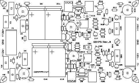
The picture shows the component print of the PCB. Of course you can't use it for anything except for an overview. Please download the pdf-file instead if you want to see the details.
The printed circuit board is made for one or two channels if you use it for QSX Mark II. It's possible to do this pcb by yourself. Just make the layout as the schematics. The pcb have groundplane on the upper side which is essential in order to get good results but you can omit it if you want.
The solder side
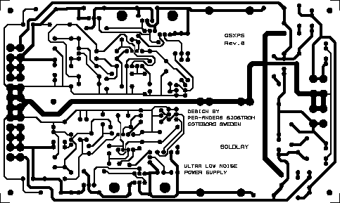
The picture shows the solder side of the PCB. Of course you can't use it for anything except for an overview. Please download the pdf-file instead if you want to see the details.
Everyone of the traces are on the solder side. The groundplane is very covering, no traces on the component side.
The component side
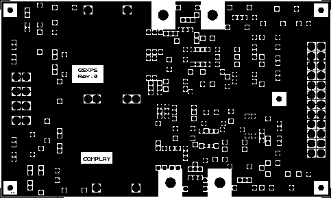
The picture shows the component side of the PCB. Of course you can't use it for anything except for an overview. Please download the pdf-file instead if you want to see the details.
Everyone of the traces are on the solder side as you can see. The groundplane is very covering, no traces on this side.
