Building directions
Patch for board Revision 0.
The new boards have unfortunately two errors.
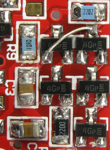
Top side
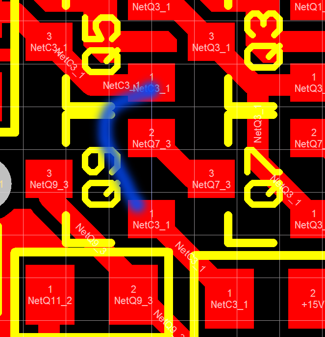
Top side patch
The base of Q9 needs to be connected to the base or collector of Q5.
Solder side, bottom side
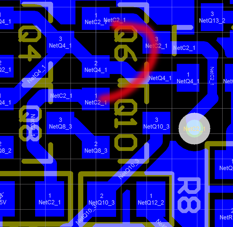
Solder side patch
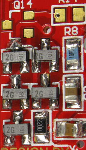
The base the collector of the Q6 needs to be connected to the base of Q10. The pcb is seen from the bottom side.
Build instructions for the prototype boards
Build in small pieces and then test
Test supply voltage is +- 15 V.
Reference voltage
Solder Q1, Q3, Q5, R4, Q6, Q4, Q2, R1, R2, R3. Then apply +- 15 volts. Measure that you have 0.6 volts between base and emitter on each transistor.
PNP emitter follower
Solder R7, Q7, Q9, R9 and Q11. R5, a tin blob. Tie the input to ground. Measure that the emitter voltage to ground at Q11. Should be 0.6V. Measure the voltage across R7. Should be 0.6V. R9 27 mV.
NPN emitter follower
Solder R6, Q8, Q10, R8 and Q12. Tie the input to ground. Measure that the emitter voltage to ground at Q12. Should be 0.6V. Measure the voltage across R6. Should be 0.6V. R8 27 mV.
Output stage
Solder Q15, R11-R13, Q16. Tie the input to ground. Measure the output voltage. Should be i mV's. Measure the voltage across the R11-R13. Should be something. Load the outout with 1kohms. Measure now the same thing.
This design is very easy to build. You should start with all low SMD parts. Solder in the electrolytic caps at last. For this solder job I recommend a good pair of tweezers. I use a type especially made for SMD. With this pair of tweezers I get a very good grip. You must also have a soldering iron with a small tip but.
Make sure if you want the class A circuit or not, Q13, Q14, R14, R15. Determine also if you want any of the R1, R2 or R3 resistors. If you don't want the input filter just short R5 with tin or a small wire.
Start with all low SMD parts
- Resistors
Transistors
Capacitors, not the electrolytic ones - Then continue with the high electrolytic caps
- Wires
