SSB-02 - The high performance SMD Diamond buffer
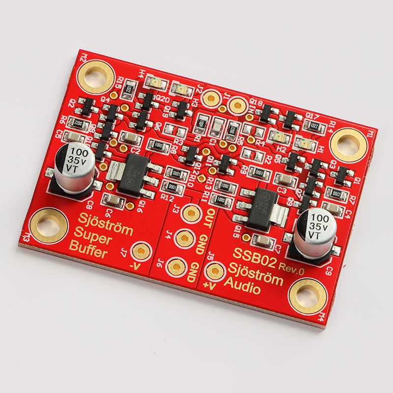
The picture shows the buffer. Click on the picture on order to get an larger view.
The performance is very good. See technical data!
Interesting features
- No global feedback.
- The pcb fits virtually any SOT23 small signal transistor and almost any SOT223 power transistor.
- The emitter loads have cascodes in order to increase linearity.
- SMD caps, including electrolytic caps.
- SMD parts which makes the buffer very small and thin.
- Bias network using red LED's.
- Input LP-filter if you have problems with RF interference, if not just omit it.
- Crossover distortion reducer for the opamp. This is a popular circuit in the DIY community.
- Useful for anything as long as power supply voltage is within limits and load not to heavy.
- Professional pcb with groundplane which establish good cooling and shielding.
Background
This type of buffer is called "diamond buffer". The name comes from the shape of the circuit and is patented, US patent 3302039, filed in 1964 . The name "Jung Super Buffer" (from his article which can't be found) has also been seen in the DIY audio comminuty. Many IC's have this diamond buffer, LT1223, BUF634, LME49600 and many more.
This buffer can be used in a preamp as line stage without gain, as a buffer for DAC's and CD-players. You can also use it for driving headphones. The buffer is rather small and very thin so it can be placed in narrow spaces.
There are lot's of good info out there on this subject. Walter Jung has written a couple of good articles and one of them is about this particular buffer. In fact his article is THE best for a normalDIY'er.
Reference articles
Realizing High Performance: Buffers (Part I) (can't be found but I have it.)
Realizing High Performance: Buffers (Part II) (can't be found but I have it.)
The ancient LH0002 is also a simple diamond buffer. The equally ancient LH0033 consists of a JFETbuffer.
AN-47 from Linear is a big document, very well written. Look especially at page 45-47. Those pages describes a discrete diamond buffer.
AN-227 from Texas Instruments is also worth reading.
This Texas document has also a part about diamond buffers.
The schematics
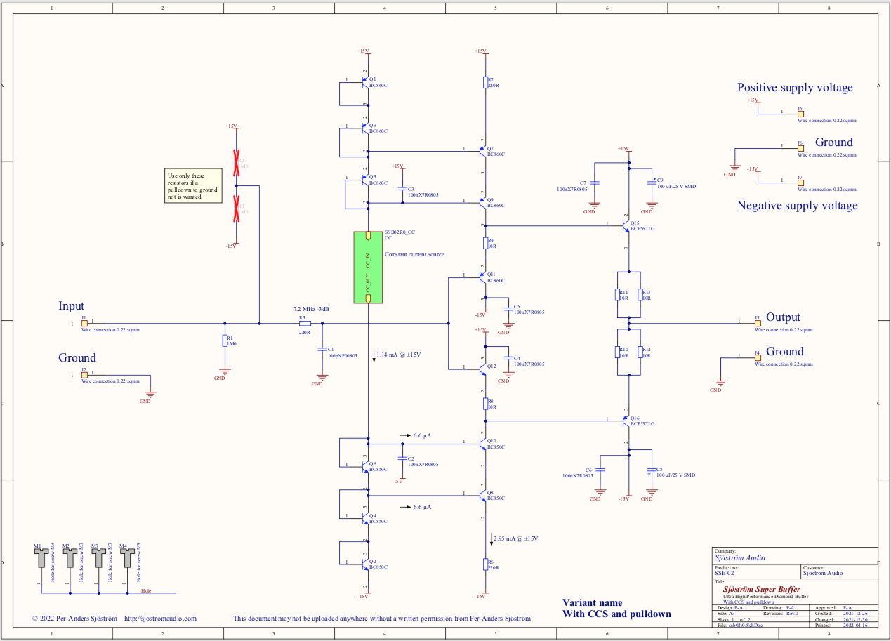
The picture shows the page 1of the schematics of the buffer. Please download the pdf-file if you want to see the details.
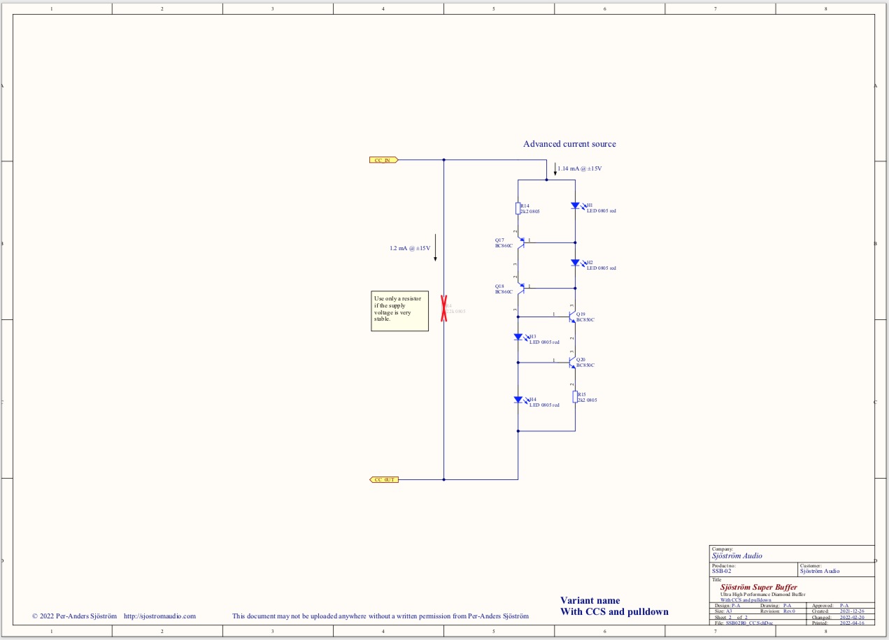
The picture shows the page 2 of the schematics of the buffer and shows the LED bias network. Please download the pdf-file if you want to see the details.
Ciruit description
The circiuit is to 95% based on the SSB01. 1I have chosen to use current generators with cascodes as emitter loads. How much good the cascodes do is unknown at the moment. The only obvious disadvantage is a little bit reduced output voltage swing, otherwise only positive things.
LED bias network
The old design SSB01 used a plain resistor to set the bias through the Q1, Q3, Q5 and Q2, Q4, Q6 but the disadvantage is that the circuit is more sensitive against varying supply voltage. The LED circuit (see page 2 of the schematic) is a low noise current source formed by two halfs consisting of cascoded current source where the LED serves as a voltage reference. Red colour is recommended but some resistors need to be recalculated if the same quiesent currents are wanted.
The current in the first stages is set by Q1, Q3 and Q2, Q4 along with R6 and R7. Transistors are used as diodes just to make it simpler when it comes to ordering parts. The current is 0.65/220 = 3 mA and the output stage will have approx. 4-6 mA.
Class A in the buffer
The max current is set by the max allowable power dissipation of the transistors. The small SOT23 types can take 310mW or so and the SOT223, output transistors can dissipate 1.3 W but not in this application I imagine. More current mean slightly higher speed. I have experimented with different settings but it becomes more difficult an unpredictable with higher settings. I support only the setting I have. The rest is left up to you.
Input filter
The input filter R5, C1 may be necessary if you are having trouble with RF interference. The values can be set to almost anything. The frequency is calculated by f= 1/(2*pi*R5*C1). -3 dB limit, see technical data below.
No current limitation
Please note that this buffer has no current limitation in order to protect the circuit so a short circuit may damage the output transistors. The buffer is intended to be used in controlled environments. If your load is unknown you may add a resistor at the output, 220 ohms or higher.
The pcb layout
The component side, top side


Click on the picture to see a preview of the pcb.
The printed circuit board is made for one channel. It requires stabilized power supply with ± 12-15 V.
The pcb have groundplane on the bottom side and partly on the top side, which is essential in order to get good results.
Almost everyone of the traces are on the component (top) side. The groundplane on the bottom side is very covering, only a few traces are there.
The bottom side

The picture shows the bottom side of the PCB. 95 % or even 99 % is covered with a ground plane and the only thing to solder on this side are the wires.
Building directions
Build in small pieces and then test
The experience solder everything in no particular order but if the board is hand soldered, then wait to the big electrolytic caps to the last.
The less experenced is recommned to divide the completion in steps.
Test supply voltage is +- 15 V.
Reference voltage
Solder Q1, Q3, Q5, R4, Q6, Q4, Q2, R1, H1-H4, R14, R15, Q17-Q20.Then apply +- 15 volts. Measure that you have 0.6 volts between base and emitter on each transistor. Measure across R14 and R15, should be 1.0-1.2 V (= 500 µA). The total current of the LED bias should be 1.0-1.2 mA.
PNP emitter follower
Solder R7, Q7, Q9, R9 and Q11. Turn on the power. Tie the input to ground. Measure that the emitter voltage to ground at Q11/Q12. Should be 0.60-0.65 V. Measure the voltage across R7. Should be 0.60-0.65V. Voltage across R9 = 25-27 mV.
NPN emitter follower
Solder R6, Q8, Q10, R8 and Q12. Tie the input to ground. Turn on the power. Measure that the emitter voltage to ground at Q12. Should be 0.60-0.65V. Measure the voltage across R6. Should be 0.60-0.65V. R8 = 27 mV.
Remove the short to the input. Measure the voltage over R1. Should be less then ±500 mV. This is a random voltage due to the ratio between the current gain Hfe in Q11 and Q12
Output stage
Solder Q15, R11-R13, Q16. Tie the input to ground. Turn on the power. Measure the output voltage. Should be ± 0-10 mV's. Measure the voltage across the R11-R13. Should be 20 mV. Load the output with 1kohms. Measure now the same thing.
Big bang method
Start in this order, most practical. Start with small parts then finish with big caps and wires.
- Transistors, the small ones SOT23
- Resistors
- Capacitors, not the electrolytic ones
- Transistors, the big ones SOT223
- Then continue with the high electrolytic caps
- Wires
Check the finished amp
Short the input. Apply voltage and check the output voltage. Measure the DC voltage at the output. It should be the specified offset voltage, a couple of millivolts.
Measure the quiescent current.
Connect a signal source to the input, either music or from a signal generator. The reproduction should be flawless using headphones or oscillscope. If headphones is to be used, insert to begin with 1 kohm in series just for protection
The whole buffer is ready.
Good luck and happy listening.
Feel free to post pictures and reviews if you want. I don't mind to publish this on facebook and instagram. Send the material to me first though.
Click on the picture to see a preview of the pcb.
Technical data
| Frequency response: | 0 Hz - 100 MHz(?), more than 20 MHz |
| Frequency response with input filter | 0 Hz - 7.2 MHz, -3 dB |
| Power bandwidth at 7 Vrms, 50 ohms: | 0 Hz - 100 MHz(?), more than 20 MHz |
| Equivalent input noise: | 0,6 µV |
| Signal to noise ratio: | 124 dB at 1 V out |
| Dynamic headroom: | 141 dB |
| Distortion: | 0,005% (more detailed measurements will come) |
| Slew rate: | 3000 V/us |
| Step response: | Perfect without overshoot |
| Gain: | 0.999 (0 dB) |
| Input impedance: | >1 Mohms, pullup, pulldown resistors not included. |
| Output impedance: | 2.5 ohms |
| Output current: | 1 A peak |
| Supply voltage: | +- 6 to 18 V DC with chosen transistors |
| Current consumption: | 9.0 mA typical at ±15 Volts supply voltage |
| Dimensions: | 21.7 (0.852") x 32.0 (1,261") mm |
Review of my QRV08 headphone amplifier
Neurochrome has tested my QRV08 headphone amplifier which has the same output stage. This test can be seen as a hint of the performance of the buffer alone.
