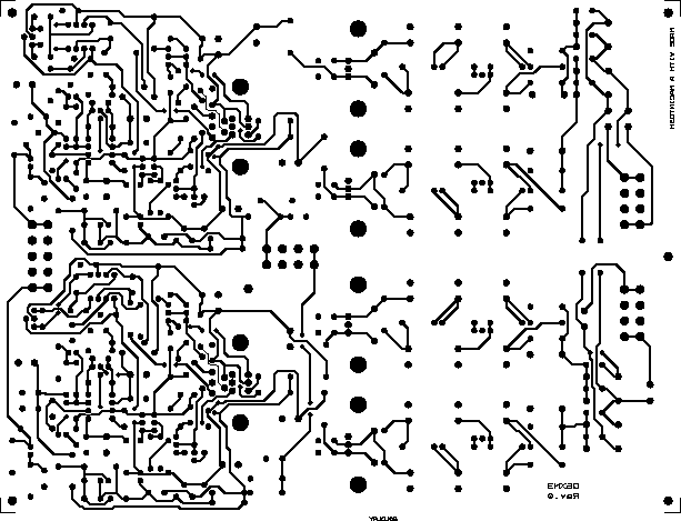
The pcb layout
The component print
The picture shows the component print of the PCB. Of course you can't use it for anything except for an overview. Please download the pdf-file instead if you want to see the details.
The printed circuit board is made for two channels. It's possible to do this pcb by yourself. Just make the layout as the schematics. As you can see I have done it. The pcb have groundplane on the upper side (not shown in pictures) which is essential in order to get good results. I haven't made it easy for switching pickup. I gather you will use only one type and also trim for this type.
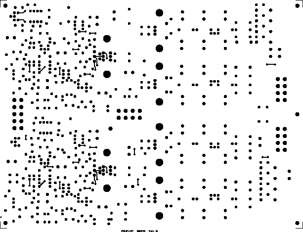
The solder side
The picture shows the solder side of the PCB. Of course you can't use it for anything except for an overview. Please download the pdf-file instead if you want to see the details.
Almost everyone of the traces are on the solder side. The groundplane is very covering, only a few traces on the component side.
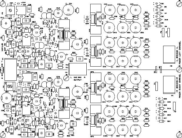
The component side
The picture shows the component side of the PCB. Of course you can't use it for anything except for an overview. Please download the pdf-file instead if you want to see the details.
Almost everyone of the traces are on the solder side as you can see. The groundplane is very covering, only a few traces on this side.
